2025 Top Trends in Printed PCB Board Technology and Innovations You Need to Know
As we approach 2025, the landscape of printed PCB board technology is poised for revolutionary changes that will shape various industries. Dr. Emily Chen, a leading expert in electronics manufacturing and a prominent figure in the printed PCB board sector, emphasizes the significance of these advancements by stating, "The future of printed PCB board technology lies in innovation, efficiency, and sustainability. We are on the brink of an era where smarter designs will lead to unprecedented possibilities."
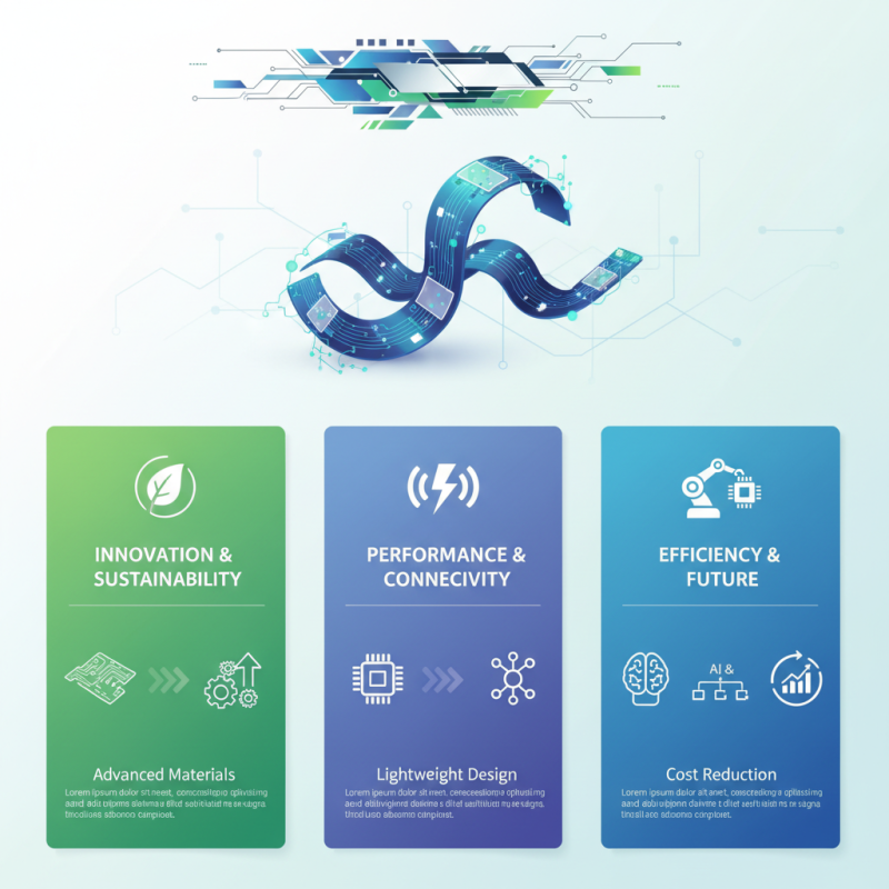
The upcoming trends in printed PCB board technology not only promise enhanced performance but also drive the shift towards greener manufacturing practices. As the demand for lightweight, high-speed connectivity grows, innovations such as flexible PCBs and advanced materials will enable the industry to meet these challenges head-on. Furthermore, the integration of Artificial Intelligence and automation into PCB design and production processes will optimize efficiency and reduce costs, allowing manufacturers to remain competitive in a rapidly evolving market.
In this article, we will explore the top trends and innovations that will define the printed PCB board industry in 2025, shedding light on the technologies that are set to revolutionize how circuits are designed, produced, and utilized across various applications.
Key Innovations Shaping the Future of Printed PCB Technology in 2025
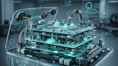
As we move towards 2025, the landscape of printed PCB technology is poised for groundbreaking advancements that will redefine the electronics industry. Key innovations such as high-density interconnects (HDI) and advanced materials like flexible and high-temperature PCBs are becoming increasingly significant. These innovations not only support the miniaturization of devices but also enhance their performance, enabling more complex functionalities within smaller footprints.
Tips: When selecting PCB materials, it's essential to consider factors like thermal stability and flexibility, especially for applications in automotive and wearable technology where environments can be demanding.
Moreover, the integration of smart technologies into PCBs is on the rise. This includes the use of embedded components and sensors that allow for real-time monitoring and data collection. Such advancements will lead to smarter, more efficient devices that can adapt and respond dynamically to user needs.
Tips: For designers, staying updated with the latest simulation tools can aid in anticipating design challenges and optimizing layouts for high-speed applications, thus reducing development time and cost.
2025 Top Trends in Printed PCB Board Technology and Innovations You Need to Know
| Trend |
Description |
Impact |
Year Introduced |
| Flexible PCBs |
Increase in the use of flexible PCB technologies for wearable devices. |
Enhanced adaptability in design and increased modularity. |
2023 |
| High-Frequency PCB |
Development of PCBs that can operate at higher frequency ranges for 5G applications. |
Improved signal integrity and reduced electromagnetic interference. |
2024 |
| Eco-Friendly Materials |
Shift towards biodegradable and recyclable materials for PCB manufacturing. |
Reduction in environmental impact and compliance with regulations. |
2025 |
| 3D Printing Technology |
Adoption of 3D printing methods for faster prototyping and production. |
Reduced lead times and increased customization. |
2024 |
| Autonomous Manufacturing |
Integration of AI and robotics in PCB manufacturing processes. |
Higher efficiency and accuracy in production. |
2025 |
Sustainability Trends and Eco-friendly Materials for PCBs in 2025
As the demand for eco-friendly solutions continues to rise, the printed circuit board (PCB) industry is witnessing a significant shift towards sustainability. A recent report by market research firm Research and Markets indicates that the global eco-friendly PCB market is expected to grow at a compound annual growth rate (CAGR) of 7.4% from 2023 to 2028. This growth reflects the increasing emphasis on environmentally responsible manufacturing processes and the use of sustainable materials throughout the production cycle.
In 2025, innovations in sustainable PCB materials are set to take center stage. Manufacturers are increasingly adopting bio-based resins and recyclable materials, which not only reduce the carbon footprint but also minimize waste. According to a study published in the Journal of Cleaner Production, the integration of eco-friendly materials can decrease energy consumption in the PCB fabrication process by up to 30%. Additionally, advancements in green chemistry are leading to the development of halogen-free laminates and lead-free solder, which are crucial for minimizing the environmental impact of electronic waste.
Moreover, regulatory pressures and consumer awareness are propelling the transition towards greener practices in the PCB sector. The European Union's RoHS (Restriction of Hazardous Substances) directive highlights the importance of reducing hazardous materials in electronics. By 2025, the industry is expected to see a comprehensive adoption of these eco-friendly standards, with an estimated 80% of PCB manufacturers incorporating sustainable practices into their operations. This shift not only aligns with global sustainability goals but also enhances the competitive edge of businesses committed to environmentally responsible production.
2025 Trends in Printed PCB Technology
Advancements in PCB Manufacturing Processes and Techniques
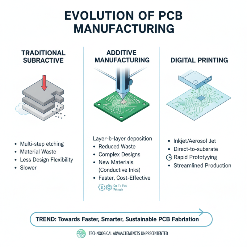
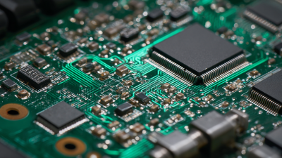
The evolution of Printed Circuit Board (PCB) manufacturing processes is paving the way for unprecedented advancements in technology. One of the most significant trends is the transition to additive manufacturing techniques, which enable the creation of highly complex PCB designs with reduced material waste. This approach not only enhances the design flexibility but also allows for the integration of new materials such as conductive inks, which can significantly lower production costs and time. The shift towards digital printing methods is transforming traditional PCB fabrication, with companies increasingly adopting these innovative processes to streamline production.
Another notable advancement is the adoption of advanced surface mount technology (SMT) that has facilitated the miniaturization of components. With the demand for smaller, more efficient electronic devices on the rise, manufacturers are focusing on improving assembly techniques to accommodate high-density PCBs. Additionally, the use of machine learning and artificial intelligence in quality control processes has emerged, enabling real-time monitoring and defect detection during manufacturing. These technologies not only enhance productivity but also ensure greater reliability and consistency in PCB production, supporting the ongoing trend towards high-performance electronics across various industries.
Integration of Smart Technologies in Printed Circuit Boards
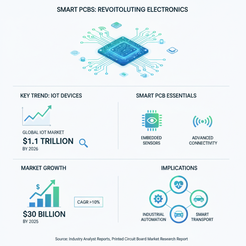
The integration of smart technologies into printed circuit boards (PCBs) is revolutionizing the electronics landscape, with significant implications for various industries. The growing trend of IoT devices is a driving force behind this integration, as reported by industry analysts predicting that the global IoT market will grow to $1.1 trillion by 2026. Smart PCBs are becoming essential components of these devices, enhancing their functionality through embedded sensors and advanced connectivity features. Data from the "Printed Circuit Board Market Research Report" indicates that the smart PCB market is expected to reach $30 billion by 2025, reflecting a compound annual growth rate (CAGR) of over 10%.
In the pursuit of smarter PCBs, manufacturers are now focusing on integrating multifunctional capabilities while maintaining their traditional roles. One major innovation involves the use of flexible and stretchable electronics, allowing PCBs to conform to various shapes and surfaces. This flexibility is crucial for wearable technology and medical applications, where form factor plays a vital role. Furthermore, the embedding of artificial intelligence (AI) processes within PCBs promises to enable predictive maintenance and enhance the efficiency of electronic systems.
**Tips:** When designing smart PCBs, consider the thermal management of embedded components, as excessive heat can dramatically affect performance. Additionally, prioritize modular designs to enhance repairability and upgrade potential, which can significantly extend the lifecycle of electronic products. Engaging in continuous market analysis will also aid in anticipating trends and aligning designs with future technology needs.
Emerging Applications of Printed PCBs in Various Industries for 2025
As we look forward to 2025, printed circuit boards (PCBs) are set to revolutionize various industries with their innovative applications. The integration of printed PCBs into consumer electronics, automotive systems, and healthcare devices is paving the way for significant enhancements in functionality and efficiency. For instance, in consumer electronics, the trend towards thinner and more flexible PCBs is enabling manufacturers to create sleek devices without compromising on performance. In automotive applications, the rise of electric vehicles is driving the demand for lightweight PCBs that can support advanced electric and hybrid systems, optimizing energy use while reducing weight.
Tip: When exploring new PCB technologies, assess the manufacturing capabilities closely. Understanding the technologies used in the production of PCBs can help you choose more sustainable and efficient options that meet industry standards.
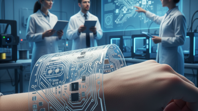
The healthcare sector is also experiencing a surge in the use of printed PCBs, particularly in medical devices and wearables. With their ability to integrate sensors for real-time monitoring, these boards offer tremendous potential for patient care and remote health management. Moreover, advancements in biocompatible materials are opening the door for innovative PCB designs that improve the reliability and safety of medical implants.
Tip: Stay updated on the latest materials and innovations in PCB technology. Innovations such as biodegradable materials can not only enhance your product’s sustainability but also appeal to a growing demographic that values eco-consciousness in their purchasing decisions.