In the rapidly evolving field of circuit board design, expertise is key. Dr. Li Wei, a renowned circuit board specialist in China, emphasizes, “Innovation in design can make or break a product's success.” The landscape of circuit board design has seen remarkable advancements. Various techniques have emerged, making the design process more efficient and effective.
Beneath the surface of these advances lies complexity. Designers must balance functionality, manufacturability, and cost. The importance of quality materials cannot be overstated. Choosing the right components can greatly impact performance. However, many designers overlook this aspect in favor of quick solutions.
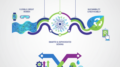
China has become a hub for circuit board design, attracting global attention. Yet, it is essential for designers to stay updated. The industry is not without challenges. As technology progresses, so does the difficulty of meeting strict design standards. This dynamic environment calls for a commitment to continuous learning and adaptation. Embracing both the innovative and the imperfect can lead to substantial growth in this field.
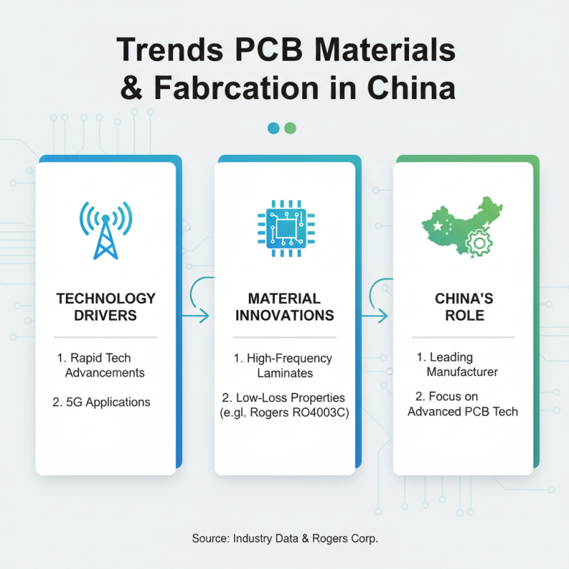
Circuit board design in China requires careful attention to detail and adherence to best practices. A critical aspect is ensuring efficient layout. Designers must consider signal integrity and minimize electromagnetic interference. Using advanced software tools can assist in achieving these goals. Yet, the learning curve can be steep. Many newcomers to the industry face challenges in mastering these tools.
Thermal management is another essential aspect. Proper heat dissipation prevents component failure and extends the board’s lifespan. Selecting suitable materials is vital. However, many designers might overlook the importance of thermal vias. Without them, overheating can lead to costly failures.
Collaboration with manufacturing partners can enhance design outcomes. Establishing open communication helps in identifying potential issues early. It fosters a culture of problem-solving. Not all designs will be perfect on the first try. Iteration is part of the process. Embracing feedback and refining designs can lead to superior results in the fast-paced electronics market in China.
| Technique | Description | Benefits | Common Applications |
|---|---|---|---|
| Via-in-Pad | A technique where vias are placed directly into the pads of components. | Reduces the footprint; enhances signal integrity. | High-density interconnect boards, RF circuits. |
| Layer Stacking | Arranging the layers in a specific order to optimize performance. | Improves EMI shielding; enhances signal routing. | Multilayer PCBs, sensitive analog circuits. |
| Controlled Impedance | Designing traces to ensure they maintain a specific impedance. | Reduces signal reflections; enhances performance. | High-speed digital systems, RF applications. |
| Thermal Management | Techniques used to maintain temperatures within limits. | Increases reliability; prevents overheating. | Power electronics, LED applications. |
| DFM and DFT | Design for Manufacturing and Design for Testability. | Simplifies production; improves testing processes. | Consumer electronics, automotive systems. |
China has emerged as a powerhouse in PCB technology, demonstrating significant advancements in recent years. Key innovations include high-density interconnections that allow for smaller, more efficient circuit boards. This development is essential for the growing demand for miniaturized electronics. Additionally, advancements in materials, such as flexible and high-frequency laminates, have broadened the application spectrum of PCBs.
Another noteworthy trend is the adoption of automated manufacturing processes. These technologies enhance precision and reduce production time. Companies also focus on sustainability, creating eco-friendly PCBs that minimize environmental impact. Despite these achievements, challenges remain. The need for skilled technicians in specialized areas and maintaining quality amidst rapid production growth is critical.
Moreover, enhancing design software remains an area for improvement. Current solutions may not fully cater to innovative design requirements. As the industry evolves, continuous learning and adaptation will be necessary for engineers. Tracking these innovations reveals a vibrant landscape ripe with potential, yet reliant on addressing existing gaps in skills and technology.
In today's competitive landscape, efficient PCB design is essential. DFM (Design for Manufacturing) and DFA (Design for Assembly) significantly impact design efficiency and cost. By incorporating DFM principles, designers can create PCBs that are easier to manufacture. This approach reduces production delays and errors. Effective DFM ensures that components are not only fit for their intended purpose but also compatible with manufacturing processes.
DFA focuses on simplifying assembly. The easier a PCB is to assemble, the higher the productivity. Prioritizing component placement can minimize the use of tools and time. It is vital to consider how each part interacts with others. However, unnecessary complexity often creeps in. Designers should strive to balance innovation with practicality.
**Tip:** Always perform a DFM review early in your project. Addressing potential issues upfront can save time in the long run.
Another consideration is the communication between design and manufacturing teams. Transparency helps identify challenges early. Iterative feedback is crucial for refining designs.
**Tip:** Schedule regular check-ins to discuss DFM and DFA elements in your PCB design. Engage with your team to pinpoint areas of improvement. Finding the balance is a constant reflection in the design process.
In recent years, China has emerged as a leader in PCB (Printed Circuit Board) materials and fabrication techniques. The rapid advancements in technology have influenced design practices significantly. Companies are now focusing on using high-frequency laminate materials to meet the growing demands of 5G applications. For instance, Rogers Corporation's data indicates increased demand for materials like RO4003C, known for its low-loss properties.
Emerging trends highlight the shift towards more eco-friendly materials and processes. Reports from research firms suggest a significant rise in demand for biodegradable substrates. This trend reflects a broader commitment to sustainability within the industry. However, the transition is not without challenges. The cost of new materials often outweighs traditional options, leading to hesitations among manufacturers.
Additionally, advanced fabrication techniques such as additive manufacturing are gaining traction. This method allows for more complex designs and reduced material waste. However, it requires substantial investment in new technologies and training. As companies adapt, balancing advancement with cost-effectiveness remains a critical issue. The journey is ongoing, and while some challenges may slow down progress, the drive for innovation in PCB design in China continues.
In the rapidly evolving field of circuit board design, advanced software tools play a crucial role. These tools facilitate high precision and efficiency in circuit layout and simulation. Designers can visualize circuit behavior before physical production, significantly reducing potential errors and issues.
Using software like PCB design applications, engineers can optimize layouts. This involves minimizing signal interference and ensuring efficient power distribution. However, relying solely on software presents challenges. It’s crucial for designers to maintain a strong grasp of fundamental principles. Over-dependence on tools may lead to overlooking basic design flaws.
Tips for optimization include focusing on layer stack-up early in the design process. Also, consider the manufacturer's capabilities when creating designs. Regularly review and update your knowledge on software features. This helps in leveraging the latest advancements effectively. Embrace feedback from prototypes to refine your design approach further. Adaptability is key in achieving optimal results.