Choosing the best PCB prototyping service in 2026 takes more than comparing quoted prices. A low-cost board can become expensive if a design flaw surfaces after assembly. The right partner helps you find problems while changes are still manageable.
This guide compares services through practical criteria: fabrication speed, layer-count options, material choices, assembly support, design-for-manufacturing feedback, and shipping transparency. It also considers whether providers explain tolerances clearly and offer useful updates when a job encounters a delay. Small details matter. A clearly labeled impedance option or a realistic lead-time estimate can prevent costly surprises.
Signal-integrity expert Eric Bogatin has emphasized, “The three most important things in signal integrity are return paths, return paths, and return paths.” That principle matters even during early prototyping, when a test board may contain high-speed signals and tight routing constraints. A quick prototype is not automatically a good one. The board still needs to reflect the electrical and mechanical demands of the final product.
No comparison can suit every engineer. A student testing a simple sensor board may value a low minimum order, while a product team may need controlled assembly and repeatable results. Provider capabilities and pricing can also change during the year. Treat rankings as a starting point, not a substitute for checking current specifications and requesting a detailed quote. This overview highlights where common services may fit, what trade-offs to inspect, and which questions deserve an answer before you upload your files.
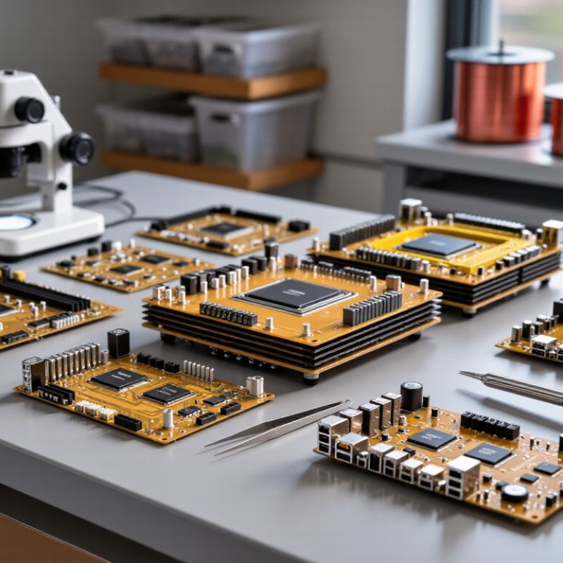
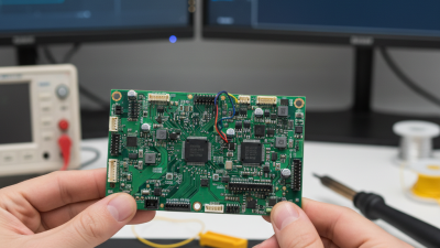
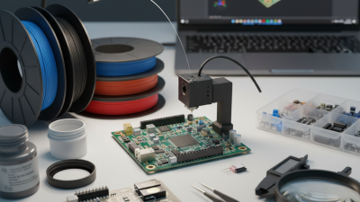
PCB prototyping services turn a circuit design into physical boards for evaluation before larger production. A typical order starts with fabrication files, layer count, board dimensions, and material details. Some providers also assemble components, letting teams test a working device rather than a bare board. Small batches are useful. They make it easier to compare revisions without committing to thousands of units.
The service matters because layout problems often appear only after fabrication. A connector may sit too close to an enclosure wall, or a fine-pitch part may be difficult to solder. Prototype runs help engineers check fit, signal behavior, thermal performance, and assembly access. Depending on the service, options may include impedance control, solder-mask colors, electrical testing, and documented inspection. Ask how file checks are handled and whether unclear footprints are reviewed by a qualified engineer. A fast quote is not the same as a technically sound review.
A useful provider should state tolerances, materials, lead times, and test limits clearly. Compare those details with the board’s actual needs, not just the lowest price. For example, a four-layer sensor board may need controlled impedance, while a simple LED board may not. Provide accurate files and a clear bill of materials; otherwise, assembly estimates can be misleading. Even careful checks may reveal an overlooked assumption in the first revision. That is frustrating, but it is part of prototyping. The aim is to learn cheaply and correct the design before production.
A PCB prototype is useful only when it tests the design you intend to build. Evaluate providers by more than headline price or advertised turnaround. Check whether engineers review Gerber files, flag clearance or annular-ring risks, and confirm the layer stack before production. Ask how they handle controlled impedance, board thickness, copper weight, and solder-mask tolerances. Details matter. A clear quote should identify tooling charges, shipping, electrical testing, and the exact revision being fabricated.
Production speed is valuable, but predictable communication can save more time. Look for a stated schedule covering file review, fabrication, inspection, and dispatch, with prompt notice if a question pauses the job. Ask what testing is included, such as continuity and isolation checks, and whether test results are available. For a high-speed design, confirm whether impedance coupons and measured data can be supplied. Compare providers using the same board files and specifications; otherwise, low quotes may reflect different assumptions. One point is easy to miss: a prototype service cannot compensate for incomplete design documentation. Even so, a careful review may catch a costly mistake before assembly. No checklist removes all risk, and I would treat unusually confident promises with some caution.
Key criteria for evaluating PCB prototyping providers
Suggested evaluation weighting, not survey results: compare providers on delivery time, fabrication quality, design-rule support, pricing transparency, order flexibility, material and stackup options, and testing traceability. Adjust the weights to fit your project’s priorities.
What Are the Best PCB Prototyping Services in 2026?
Comparing Manufacturing Capabilities, Costs, and Turnaround Times
The best service depends on what your prototype must prove. Check supported layer counts, board thicknesses, copper weights, and minimum feature sizes against your design files. A compact two-layer sensor board has different needs from a dense multilayer controller. Ask whether the quoted process includes electrical testing, solder mask, and the finish you need. These details affect both usability and price.
Turnaround estimates can be misleading if they start only after design review. Compare the full timeline, including file checks, fabrication, and shipping. Request separate prices for standard and expedited production, and confirm what happens if files need correction. Speed is not everything. A low quote may omit a useful inspection step, while an expensive option may offer capacity your design does not need. That trade-off is easy to miss.
Tips: Send clean fabrication files and a clear stack-up request. Ask for a written breakdown of setup fees, board quantity, shipping, and testing. For a first run, consider a small batch and inspect the boards before ordering more. A practical lesson: estimates are only as reliable as the specifications behind them. I would still leave room for one schedule slip; prototype plans rarely behave perfectly.
A practical comparison of common prototype-service profiles. Cost and production-time figures are indicative planning ranges, not live quotes or rankings.
| Service Profile | Best For | Typical Manufacturing Capabilities | Indicative Fabrication Time | Indicative Cost | Main Trade-Off |
|---|---|---|---|---|---|
| Economy Offshore Prototype | Non-urgent design checks, hobby projects, and early engineering samples. | Typically 2–4 layers; FR-4; common copper weights and surface finishes; standard design-rule limits. | About 5–10 business days, before shipping. | About US$5–25 for five 100 × 100 mm, 2-layer boards. | Lowest fabrication price, but international shipping and customs can extend total delivery time. |
| Standard-Turn Prototype | Routine product development when moderate lead time and cost are acceptable. | Commonly 2–6 layers; FR-4; plated through-holes; solder-mask and finish choices vary by order. | About 3–6 business days, before shipping. | About US$15–60 for the same 5-board, 2-layer reference order. | More schedule flexibility and options than economy service, with shipping location still affecting delivery. |
| Rapid-Turn Local or Regional Service | Hardware teams facing a deadline, design revisions, or a need for faster support. | Usually conventional 2–8-layer prototype work; expedited processing may be available for supported materials and designs. | About 1–3 business days for fabrication; shipping time is additional. | About US$50–180 for the same reference order; expedited options may cost more. | Shorter production windows and easier regional logistics, generally at a higher board price. |
| Advanced HDI or Specialty Prototype | Compact designs, fine-pitch components, dense routing, or unusual electrical and mechanical requirements. | May support microvias, blind or buried vias, finer lines and spacing, controlled impedance, or specialty laminates; availability is design- and facility-dependent. | Often about 5–15 or more business days, depending on stack-up and process complexity. | Usually quote-based; commonly several times the price of a basic 2-layer board. | Enables more demanding designs, but requires design-rule review and is not directly comparable with a basic-board price. |
Basis and caveat: The reference price assumes bare-board fabrication for five 100 × 100 mm, 2-layer FR-4 boards with standard specifications. Assembly, shipping, taxes, special finishes, and rush fees are excluded. Actual capabilities, prices, and lead times depend on the board files, order quantity, destination, and production schedule; confirm them with a current quotation.
Choosing a PCB prototyping service starts with your next production step, not the lowest prototype quote. Grand View Research valued the global PCB market at USD 76.2 billion in 2023 and projected a 5.4% compound annual growth rate from 2024 to 2030. That growth makes capacity and repeatability worth checking early. Ask whether the service can build your planned layer count, line width, and material, then scale the same stack-up for a pilot run. A fast sample helps. A consistent process matters more.
Send the fabricator your fabrication notes and ask for a design-for-manufacturing review before ordering. Look for specific feedback on annular rings, drill sizes, copper spacing, and panelization—not just a generic “files approved.” For a board with controlled impedance, confirm how the provider calculates and verifies trace geometry. Request test documentation, such as electrical test results, and clarify how revisions are tracked. These details can prevent a board that looks right but fails during assembly. The IPC-6012 qualification and performance specification is one useful reference for rigid-board requirements; confirm the applicable class and acceptance criteria for your project. A polished portal is not proof of process control. I would still compare the first article with the released files, line by line.
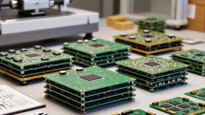
A PCB prototype begins with more than a pile of design files. The fabrication team checks Gerber or ODB++ data, the bill of materials, and assembly coordinates for mismatches. A rotated component or missing footprint can stop a build before the board reaches the production line. Small details matter.
Before fabrication, engineers review the layer stack-up, trace widths, clearances, drill sizes, and solder mask openings. They may flag copper too close to a board edge or a connector footprint that leaves little room for assembly. Clear feedback helps designers correct problems early, though review tools cannot catch every design mistake. Some details still slip through.
Once approved, the board is fabricated, assembled, and inspected. Testing may include electrical continuity checks, visual inspection, and power-up or functional tests based on the design. Ask what each test covers, and request results tied to the prototype batch. A board that passes a basic continuity check may still fail under real operating conditions. That gap is worth considering. If testing reveals a fault, the team can share measurements or images, helping the next design revision address the actual cause rather than guesswork.