Skip to content

2026 Best PCB Prototyping Techniques for Efficient Product Development

In the fast-paced world of electronics, PCB prototyping has become a vital aspect of product development. According to a report by MarketsandMarkets, the PCB prototyping market is projected to reach $12 billion by 2026. This reflects the growing demand for rapid and efficient prototyping techniques. Industry expert Dr. Emily Chen emphasizes, "The ability to iterate designs quickly is fundamental in today's competitive landscape."

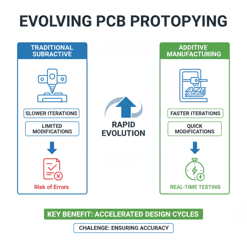
As companies strive to innovate, they require methods that reduce lead times and enhance design flexibility. Traditional approaches often fall short, leading to increased costs and delayed timelines. The shift toward advanced techniques such as 3D printing and automated assembly highlights a need for adaptable solutions. There is still room for improvement, as many firms struggle to integrate new technologies seamlessly into their workflows.

Moreover, many engineers confront challenges, like limited knowledge on the latest tools. The gap in skills can hinder the benefits that PCB prototyping offers. Ultimately, embracing innovation necessitates a commitment to ongoing learning and adaptation. Identifying these imperfections may pave the way for enhanced efficiency in product development.

2026 Best PCB Prototyping Techniques for Efficient Product Development

Current PCB Prototyping Challenges in Product Development

Current PCB prototyping challenges can complicate product development. Time constraints often lead to rushed designs. This pressure can result in errors. A minor mistake in PCB layout might delay the entire project. Designers must balance speed and quality. Finding the right materials is another hurdle. Many options have different properties and costs. Choosing incorrectly can lead to failures down the line.

Tips: Always review your design multiple times. Small errors can be costly. Feedback from colleagues can provide fresh perspectives. Consider running simulations before physical prototyping to identify issues early.

Another challenge is managing communication among teams. Engineers, designers, and manufacturers need to align. Miscommunication can lead to significant setbacks. Sometimes, there’s a disconnect between expectations and reality. Ensuring clear and open communication channels is crucial. Regular updates and meetings can minimize misunderstandings.

Tips: Use visual aids to clarify complex ideas. Simple sketches can bridge gaps in understanding. Establish a centralized platform for all project documents. This keeps everyone informed and engaged.

Overview of Traditional PCB Prototyping Techniques

Traditional PCB prototyping techniques have long been the backbone of electronics design. One of the most common methods is manual routing. Designers create traces by hand, which allows for high customization. However, this process is time-consuming and prone to errors. Careful attention is required to avoid mistakes that could lead to circuit failures.


Another widely-used technique is photo etching. In this method, a photosensitive film is applied to copper-clad boards. It offers better precision than manual routing. Yet, this process can be messy and complicated. Proper exposure and development stages are crucial. If done incorrectly, the results can be unsatisfactory, and rework is often needed.


Laser cutting is gaining traction for PCB prototyping. It provides quick and accurate cuts without damaging the substrate. However, it also requires careful calibration. Mistakes in settings can lead to wasted materials. The balance between speed and accuracy remains a challenge for many. Each traditional method has its benefits but also its drawbacks, prompting continuous reflection and improvement in PCB design processes.

Emerging Technologies Impacting PCB Prototyping

Emerging technologies are reshaping PCB prototyping, offering new ways to enhance product development. 3D printing, for example, enables rapid prototyping of complex designs. Reports indicate that 3D printing in electronics will grow at a compound annual growth rate of 23.7% through 2025. This technology allows for quicker iterations and reduces costs significantly.

Another key technology is artificial intelligence (AI). AI can optimize design processes and predict potential failures. Recent studies show that using AI can cut prototyping time by up to 30%. However, implementing AI can be challenging. Many teams struggle with integrating it into existing workflows. This can slow down progress rather than speed it up.

Tip: Start with small AI tools to test their effectiveness. Don’t rush into full integration. Organizations may also consider investing in simulation software. This can help visualize designs before physical prototypes are built. Yet, ensure your team is trained properly. Lack of knowledge can lead to costly mistakes.

Best Practices for Efficient PCB Design and Prototyping

Efficient PCB design and prototyping are crucial for rapid product development. According to industry reports, companies that adopt effective PCB prototyping techniques can reduce time to market by up to 30%. This showcases the importance of an agile approach in design iterations. Quick prototyping enables engineers to test concepts early and make necessary adjustments.

One essential practice is utilizing advanced simulation tools. These tools help predict potential failures before physical prototypes are made. However, not all designers leverage these resources effectively. Many still rely on traditional methods, which can lead to delays. A significant percentage of prototypes get redesigned multiple times due to overlooked design flaws. This inefficiency can increase costs and lengthen project timelines.

Additionally, collaboration among team members is vital. Cross-functional teams ensure that design, manufacturing, and testing phases align. Yet, communication gaps can still occur, resulting in misaligned expectations and wasted efforts. Implementing regular check-ins can address these gaps. Ultimately, embracing a streamlined approach and learning from each iteration can drive better results in PCB prototyping.

2026 Best PCB Prototyping Techniques

This bar chart illustrates the efficiency levels of various PCB prototyping techniques based on speed, cost, and material usage. The data showcases common practices in the industry to aid engineers in selecting the most effective methods for product development.

Future Trends in PCB Prototyping for Enhanced Product Development

2026 Best PCB Prototyping Techniques for Efficient Product Development

The landscape of PCB prototyping is evolving rapidly. Designers are increasingly adopting additive manufacturing for faster iterations. This technique allows for quick modifications, enabling teams to test ideas in real time. However, accuracy can sometimes be a concern. Rapid design changes might lead to errors if not carefully checked.

Additionally, AI-driven tools are becoming popular. They help automate the design process and enhance efficiency. Yet, reliance on these tools can lead to complacency. Designers must ensure they understand the basics. Ignoring foundational knowledge might cause more significant issues later on.

Sustainability is also a crucial topic. Eco-friendly materials are gaining traction in PCB prototyping. They minimize environmental impact but may come with performance trade-offs. It's essential to strike a balance between sustainability and functionality. Decisions should be made carefully, reflecting broader goals in product development.