Skip to content

How to Design Printed Circuit Boards for Beginners and Experts

In the evolving world of electronics, the significance of printed circuit boards (PCBs) cannot be overstated. These intricate boards serve as the backbone of virtually all electronic devices, from simple gadgets to complex systems. For both beginners embarking on their journey in electronics and seasoned experts looking to refine their skills, understanding the art and science of PCB design is crucial. This article aims to explore the fundamental principles and advanced techniques involved in creating efficient and effective printed circuit boards.

As we delve into the world of PCB design, we will cover essential topics that cater to varying levels of expertise. Beginners will benefit from an introduction to the basic components and layout considerations, while experienced designers will gain insights into advanced practices that enhance performance and reliability. The goal is to equip readers with a comprehensive understanding of the design process, enabling them to construct robust and innovative printed circuit boards that meet the demands of contemporary technology. Whether you are designing a prototype for a new invention or maximizing an existing project, mastering PCB design is a vital step towards electronics proficiency.

How to Design Printed Circuit Boards for Beginners and Experts

Understanding the Basics of Printed Circuit Design

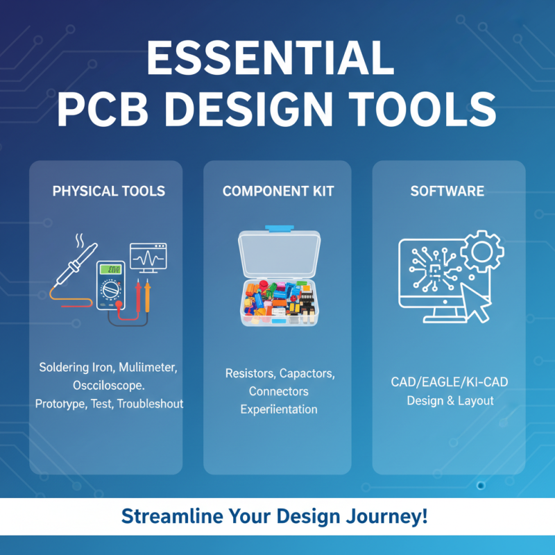
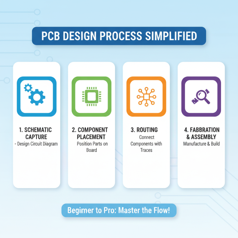
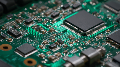
Understanding the basics of printed circuit design is crucial for both beginners and experts alike. A printed circuit board (PCB) serves as the backbone of electronic devices, connecting different components and facilitating their interactions. The design process starts with creating a schematic diagram that illustrates the electrical connections between components. This diagram serves as the blueprint for the physical PCB layout, which must accommodate space constraints and electrical properties such as impedance and thermal management.

**Tips:** When starting the design process, ensure your schematic is clear and organized. Use consistent symbols and labeling to avoid confusion later in the layout stage. Additionally, keep in mind the physical constraints of the PCB; components should be arranged logically to minimize routing complexity and reduce signal interference.

Once the schematic is complete, move on to the PCB layout. This involves placing the components on the board and routing the connections between them. It's essential to follow design best practices such as maintaining adequate trace widths, utilizing ground planes for electromagnetic compatibility, and keeping signal traces as short as possible. Pay attention to the design rules provided by your PCB design software to avoid errors that could lead to costly prototyping mistakes.

**Tips:** Regularly validate your design with simulation tools that check for electrical integrity. Additionally, consider thermal management during your layout to prevent overheating of components. An effective layout not only improves performance but also ensures reliability for the operational lifetime of the device.

How to Design Printed Circuit Boards for Beginners and Experts - Understanding the Basics of Printed Circuit Design

Dimension Description Importance
Layer Count Number of conductive layers in PCB design. Determines complexity and functionality.
Trace Width Width of the copper traces connecting components. Affects current-carrying capacity and signal integrity.
Board Thickness The thickness of the PCB material. Influences durability and stiffness of the PCB.
Component Placement Arrangement of electrical components on the PCB. Impact on assembly, performance, and functionality.
Via Type Holes used for connecting traces across layers. Affects signal routing and board density.

Essential Tools and Software for PCB Design

How to Design Printed Circuit Boards for Beginners and Experts

When embarking on the journey of printed circuit board (PCB) design, having the right tools and software is crucial for both beginners and experienced designers. Essential tools include a reliable soldering iron, multimeter, and oscilloscope. These physical tools allow designers to create prototypes, test circuits, and troubleshoot issues effectively. Additionally, using a toolkit that offers a variety of components, such as resistors, capacitors, and connectors, can greatly enhance the design process, enabling users to experiment with different circuit configurations.

On the software side, PCB design programs play a significant role in streamlining the design process. Many software options provide intuitive user interfaces and robust features, such as schematic capture, layout design, and simulation capabilities. These applications enable designers to visualize their circuits, optimize layouts for performance, and ensure manufacturability. For beginners, focusing on software with built-in tutorials and community support can facilitate learning while experienced users may appreciate advanced features like automated routing and component libraries that save time and minimize errors.

Step-by-Step Guide to Creating Your First PCB Layout

How to Design Printed Circuit Boards for Beginners and Experts

Creating your first PCB layout can seem daunting, but breaking it down into manageable steps can streamline the process and make it accessible for both beginners and seasoned professionals. A foundational aspect of PCB design begins with understanding the basic components and layout principles. According to a report by IPC, the global electronics industry is projected to reach $2.5 trillion by 2025, highlighting the ever-growing need for skilled PCB designers. This underscores the importance of a thorough understanding of the design process, which typically includes schematic design, component placement, and routing.

In the schematic design phase, it’s crucial to create a clear and organized representation of your circuit using software tools tailored for PCB creation. Once you have a solid schematic, the next step is component placement. Optimal placement can significantly influence a board’s electrical performance and signal integrity. A study published in the Journal of Electronic Materials suggests that strategic component arrangement can reduce interference and enhance functionality, supporting the theory that both aesthetic and practical considerations play vital roles in PCB design.

Finally, routing the traces between the components requires attention to detail and adherence to electrical guidelines. Proper trace width and clearance are essential to ensure current flows efficiently without overheating, while also preventing potential short circuits. According to the ANSI/IPC-2221 standard, following industry design rules enhances reliability and safety, which is paramount for any PCB application. By following these steps and leveraging industry research, both learners and experts can navigate through PCB design with confidence.

Advanced Techniques for Experienced PCB Designers

For experienced PCB designers, mastering advanced techniques is essential to push the boundaries of innovation and efficiency in circuit design. One of the most crucial aspects is optimizing signal integrity. This involves carefully selecting trace widths and lengths, as well as implementing differential pairs for high-speed signals. Using tools like simulation software can help predict and mitigate potential issues like crosstalk and reflection, thus ensuring that the PCB performs reliably under various conditions.

Another advanced technique is integrating layers effectively. Multi-layer PCBs can significantly enhance the performance of complex designs by utilizing dedicated ground and power planes. This not only improves signal integrity but also aids in thermal management. Designers should consider using vias strategically to connect layers while minimizing inductance and maintaining a compact layout. Furthermore, employing advanced routing techniques such as blind and buried vias can help in achieving a more intricate and efficient design without compromising space or performance. Understanding these intricacies and utilizing the right methodologies allows experienced designers to create sophisticated and highly functional PCBs that meet the demands of modern electronic applications.

Common Mistakes to Avoid in PCB Design Process

When designing printed circuit boards (PCBs), even seasoned professionals can trip over common pitfalls. One major mistake is failing to plan the layout effectively. A cluttered design can lead to signal interference and manufacturing difficulties. It’s crucial to create a clear hierarchy in the layout, ensuring that high-frequency components are spaced appropriately from sensitive areas. Before finalizing the design, always double-check your placement to avoid these issues.

Another common blunder is neglecting thermal management. Overheating can damage components and degrade performance, leading to costly failures. Always incorporate enough copper for heat dissipation and consider adding vias or heatsinks where necessary. A thoughtful approach to thermal design can significantly enhance the longevity and reliability of the PCB.

Tips: Always double-check your dimensions and clearances against the manufacturer’s specifications to avoid size-related issues. Additionally, consider using simulation software to visualize the electrical flow and thermal patterns before committing to a final design. Learning from these common mistakes can elevate your PCB designs, making them more functional and efficient.