In the rapidly evolving world of electronics, mastering PCB design has become an essential skill for innovators and engineers alike. As we look towards 2025, the demand for sophisticated and efficient circuit board designs is increasing, driven by the rise of innovative projects that encompass everything from smart devices to cutting-edge robotics. This guide aims to equip aspiring designers with the fundamental knowledge and techniques necessary to excel in PCB design, ensuring they are prepared to tackle the challenges of modern electronics.
Understanding the intricacies of PCB design is paramount in creating reliable and functional electronic systems. Not only does it require a solid grasp of both theoretical principles and practical applications, but it also demands creativity and foresight in addressing potential issues. Throughout this guide, we will delve into the essential components of effective PCB design, explore advanced tools and software that streamline the process, and provide insight into best practices that can elevate a project from concept to reality.
As we advance into the era of innovative electronics, developing proficiency in PCB design will open doors to a multitude of opportunities in various fields. By mastering this skill, designers will not only enhance their career prospects but also contribute to the development of groundbreaking technology that shapes our future. Join us on this journey to explore the art and science of PCB design and unlock the potential of your next electronics project.
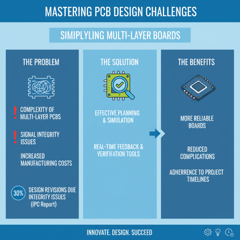
Understanding the basics of PCB (Printed Circuit Board) design is crucial for anyone looking to dive into electronics projects, especially as the industry continues to expand rapidly. According to a report by Research and Markets, the global PCB market is expected to reach $85 billion by 2025, highlighting the growing relevance of efficient PCB design in driving innovation. A well-designed PCB not only ensures the functionality of electronic devices but also enhances their reliability and performance, making it a key component for any aspiring engineer or hobbyist.
When entering the realm of PCB design, there are several critical factors to consider. First, the layout of the PCB is paramount; components must be placed strategically to minimize interference and ensure optimal signal integrity. Additionally, understanding aspects such as power distribution and thermal management can prevent failures in high-performance applications. Using simulation tools prior to production can also help in identifying potential issues early in the design process.
Tips: Always start with a schematic diagram that outlines the electrical connections between components. This foundational step simplifies the transition to PCB layout design. Furthermore, consider utilizing design rules that guide your layout process, ensuring that you adhere to industry standards and practices.
As the field of electronics evolves, the importance of mastering PCB design cannot be overstated. It not only impacts the functionality of your projects but also influences market competitiveness. Therefore, investing time in grasping these fundamental concepts will pay off in both individual projects and professional advancements within the electronics industry.
In 2025, mastering PCB design becomes crucial for engineers and hobbyists looking to push the boundaries of innovative electronics. The landscape of PCB design tools and software has evolved dramatically, enabling designers to streamline their workflows and enhance productivity. According to a recent industry report, the global PCB design software market is projected to reach USD 5.72 billion by 2026, expanding at a compound annual growth rate of 8.5%. This growth reflects an increasing demand for advanced capabilities in designing complex circuit boards for applications ranging from consumer electronics to sophisticated industrial systems.
Key tools for effective PCB design in 2025 include integrated development environments that facilitate collaboration among teams and enhance schematic capture. Cloud-based solutions are expected to gain traction, providing remote access to design files and real-time updates regardless of the team’s location. Additionally, simulation software that can predict electrical performance and thermal characteristics before physical prototyping is becoming more mainstream. Reports indicate that companies leveraging these advanced design tools report up to a 30% reduction in time-to-market, showcasing their critical role in effective PCB design processes. Understanding these tools and their functionality will empower designers to create innovative projects that meet the growing demands of technology.
This chart illustrates the usage trends of various PCB design tools in 2025. Altium Designer leads with 30% usage, followed by Eagle and KiCad with 25% and 20% respectively.
Mastering PCB (Printed Circuit Board) design is essential for anyone looking to innovate in the electronics field. The process of designing a PCB from concept to prototype involves several key steps that require both technical skill and creativity. According to recent industry data, the global PCB market is projected to reach $73.5 billion by 2025, indicating a growing demand for skilled designers who can deliver high-quality, efficient layouts for complex electronic devices.
The first step in the process is conceptualization, where the designer must outline the purpose and specifications of the PCB. This requires a comprehensive understanding of the electronic components involved and the overall functionality desired in the final product. Once the concept is established, the next phase is schematic design, where the electrical connections between components are mapped out using specialized software. This stage is crucial as it sets the foundation for the layout, influencing the board's performance and manufacturability. As per a survey by IPC, more than 60% of designers prioritize functionality and manufacturability in their initial designs, underscoring the importance of careful planning at this stage.
After completing the schematic, designers move to the layout stage, where the physical arrangement of components is designed. This step often involves iterative testing and simulation to ensure signal integrity and minimize issues such as electromagnetic interference. Once the prototype is developed, extensive testing follows to validate that the PCB operates as intended. The entire design process not only aids in producing effective electronic circuits but also contributes to the overall development cycle of electronic products, reflecting the increasing complexity of modern electronics. According to market research, the demand for high-density interconnect (HDI) boards is on the rise, expected to dominate PCB applications by 2025, showcasing the need for proficiency in advanced design techniques.
| Step | Description | Tools Required | Estimated Time |
|---|---|---|---|
| 1 | Define project requirements and specifications. | Requirements document | 1 week |
| 2 | Select components based on requirements. | Component database | 2 days |
| 3 | Create schematic diagrams. | Eagle, KiCAD | 1 week |
| 4 | Design PCB layout from schematic. | Altium Designer, DipTrace | 2 weeks |
| 5 | Run design rule checks (DRC). | PCB design software | 2 days |
| 6 | Generate Gerber files for manufacturing. | Gerber generation tool | 1 day |
| 7 | Order PCB prototypes from manufacturer. | Manufacturing service | 1-2 weeks |
| 8 | Assemble components on PCB. | Soldering tools | 1 week |
| 9 | Test and debug the PCB. | Multimeter, oscilloscope | 1 week |
| 10 | Finalize design and prepare for production. | Documentation tools | 3 days |
The journey of mastering PCB design is laden with challenges that can hinder the development of innovative electronics projects. One of the most common issues faced by designers is the complexity of multi-layer PCBs, which can introduce signal integrity problems and increase manufacturing costs. According to a report from the IPC (Association Connecting Electronics Industries), about 30% of design revisions in PCB manufacturing are a result of these integrity issues, highlighting the need for effective planning and simulation during the design phase. Utilizing tools that allow for real-time feedback and verification can significantly reduce these complications, enabling designers to create more reliable boards while adhering to project timelines.
Another significant challenge arises from component placement and the layout process. Improper placement can lead to problems such as power distribution issues, thermal management problems, and electromagnetic interference (EMI). A study by Mentor Graphics indicates that nearly 40% of PCB design failures are linked to poor layout decisions. To mitigate these risks, designers should incorporate advanced tools that provide automated design rule checks and thermal simulations, ensuring that components are optimally placed to maintain performance and reliability. Additionally, collaborating in cross-functional teams during the design phase can provide diverse perspectives that enhance problem-solving and ultimately lead to more successful PCB designs.
The rapid evolution of electronics necessitates a corresponding advancement in PCB design, a field increasingly influenced by new technologies and industry trends. As projected by the global PCB market, which is expected to reach approximately $100 billion by 2025, there will be an intensified focus on miniaturization and higher functionality in PCB designs. This trend reflects the broader demand for compact electronic devices that do not compromise on performance. Manufacturers are now exploring advanced materials such as flexible circuits and high-frequency laminates, enabling more complex and efficient designs tailored for emerging applications like 5G technology and the Internet of Things (IoT).
Additionally, sustainability is becoming paramount in PCB design. Recent reports have indicated that about 60% of manufacturers are integrating eco-friendly materials and processes to meet stricter environmental regulations and consumer demand for greener products. This shift not only addresses waste management and resource utilization concerns but also drives innovation in the manufacturing processes and materials used, such as lead-free solder and biodegradable substrates. As these trends continue to shape the landscape of electronics development, PCB designers must adapt to harness these innovations effectively, ensuring their projects are both cutting-edge and environmentally responsible.