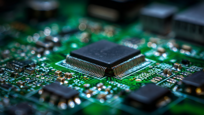
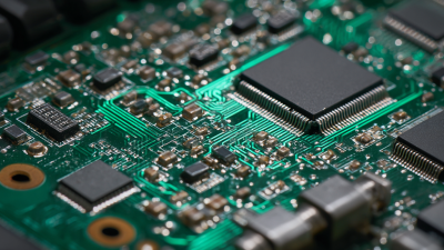
PCB fabrication is a critical process in the realm of electronics, serving as the bridge between design and implementation. At its core, PCB fabrication involves the creation of printed circuit boards, which are essential for connecting various electronic components and enabling functionality. Understanding the intricacies of PCB fabrication not only provides insight into the manufacturing process but also highlights its significance in the success of your electronics projects.
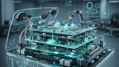
In today’s fast-evolving technological landscape, the quality and efficiency of PCB fabrication can have profound effects on the performance, reliability, and overall cost of electronic devices. From prototyping to large-scale production, each step in the fabrication process can influence design choices and project timelines. By delving into the aspects of PCB fabrication, one can appreciate how advancements in techniques and materials continue to drive innovation in electronics, opening up new possibilities for engineers and hobbyists alike. Consequently, mastering the fundamentals of PCB fabrication is essential for anyone looking to turn their electronic ideas into tangible products.
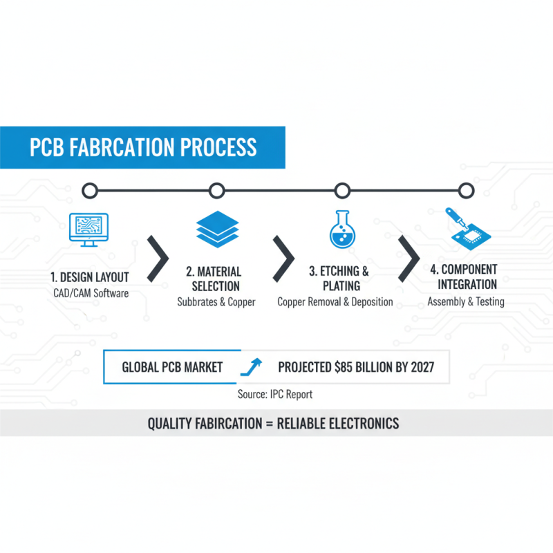
PCB fabrication is a critical process in the electronics industry, enabling the transformation of designs into tangible products. It encompasses various steps, including design layout, material selection, etching, and component integration. According to a report by IPC (Association Connecting Electronics Industries), the global PCB market is projected to reach $85 billion by 2027, driven by advancements in technology and increasing demand for electronic devices. Understanding these stages is essential for engineers and designers, as the quality of PCB fabrication directly affects the performance and reliability of electronic products.
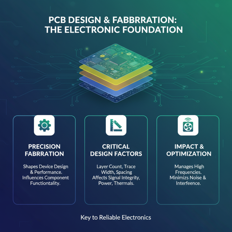
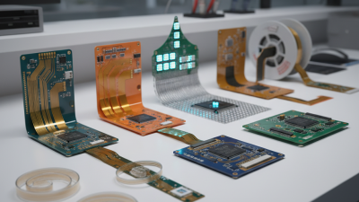
When embarking on electronics projects, it's crucial to request prototypes and test different designs before finalizing production. As highlighted by industry experts, a well-fabricated PCB can reduce the likelihood of failures, thus saving costs on revisions and delays. Additionally, selecting the right material—such as FR-4 or Rogers—plays a significant role in the functionality of high-frequency applications.
Tips: Always opt for a PCB manufacturer that uses advanced fabrication techniques to enhance the durability and longevity of your projects. Also, consider the design for manufacturability (DFM) principles to ensure a smoother production process and avoid unnecessary complications later on. Prioritizing these factors can substantially impact the success of your electronics initiatives.
The PCB fabrication process is a meticulously structured series of steps that transform a design concept into a working electronic circuit. Initially, the process begins with designing the PCB using specialized software, enabling engineers to create layouts that maximize functionality and efficiency. Following the design, the fabrication stage includes several critical steps such as photo-etching and drilling. A report from the IPC (Association Connecting Electronics Industries) indicates that the global PCB market was valued at approximately $63 billion in 2020 and is projected to grow rapidly, highlighting the increasing importance of effective fabrication processes.
Once the PCB is fabricated, it undergoes a comprehensive quality control assessment, ensuring that every component is placed accurately. The layer-by-layer arrangement, often ranging from a single layer to multilayer designs, directly influences the performance and reliability of the final product. The intricacies of this process signify its impact on electronics projects; a report from Research and Markets states that improperly fabricated PCBs can lead to higher failure rates and increased costs, underscoring the need for precision in fabrication. Understanding these steps allows engineers and project managers to optimize their designs, ultimately enhancing the reliability of their electronic products.
The materials used in PCB (Printed Circuit Board) manufacturing play a crucial role in the performance, reliability, and overall functionality of electronic devices. The most common substrate material is FR-4, a fiberglass-reinforced epoxy laminate that provides excellent insulation properties and mechanical strength. FR-4 is popular for a wide range of consumer electronics due to its thermal stability and cost-effectiveness.
However, for specialized applications such as high-frequency or high-temperature environments, alternative materials like polyimide or ceramic substrates may be used to enhance thermal performance and signal integrity.
Another key component is the conductive material used for traces, typically copper. The thickness of the copper layer, measured in ounces per square foot, directly affects the board's current carrying capacity and heat dissipation. Additionally, the choice of solder mask and surface finish materials can influence solderability and corrosion resistance, ultimately affecting the longevity and durability of electronic devices. As technology continues to advance with trends like miniaturization and increased power demands, the selection of appropriate materials will become even more critical in ensuring the efficiency and reliability of future electronic projects.
PCB fabrication involves various techniques that are essential for the production of printed circuit boards, which are the backbone of modern electronic devices. Among the most common methods are subtractive and additive processes. The subtractive method begins with a thick copper layer on the board's surface, where unwanted copper is etched away to form the desired circuit pathways. This approach is widely used due to its effectiveness for standard designs and its compatibility with mass production.
On the other hand, the additive process builds up the circuit board layer by layer, adding copper only where it is needed. This technique allows for greater design flexibility and is advantageous for creating complex circuits or when working with high-density interconnections. Additionally, advanced technologies such as automated optical inspection and lithography play significant roles in ensuring precision and reliability during the fabrication process. Each technique has its unique applications, making it essential for designers to understand their choices when embarking on electronics projects.
PCB fabrication is a crucial process that shapes the design and performance of electronic devices. The precision of PCB fabrication directly influences the functionality of the electronic components mounted on the board. When designing a printed circuit board, various factors such as layer count, trace width, and spacing must be meticulously considered. These decisions are not merely technical; they profoundly affect signal integrity, power distribution, and thermal management within the device. Effective PCB design ensures that high frequencies are managed correctly, minimizing noise and interference that could disrupt the performance of sensitive electronics.
Moreover, the materials used in PCB fabrication play a significant role in determining the reliability and efficiency of electronic products. The choice between different substrates and finishes can impact not only the performance metrics but also the longevity of the device in various environmental conditions. For instance, using high-quality materials can enhance thermal conductivity and minimize the risk of signal loss, ensuring that the electronic device operates effectively under stress. Therefore, a thorough understanding of PCB fabrication processes is essential for engineers and designers who aim to optimize their projects for performance and reliability, aligning with the intended use of the final product.