PCB fabrication is a critical process in the development of electronics, serving as the backbone of modern technology. As we delve into the intricate world of PCB manufacturing, it's essential to understand that PCB fabrication involves various stages, from design and layout to etching and assembly. This comprehensive guide offers a detailed overview of each phase, highlighting the methodologies and technologies employed in creating printed circuit boards that meet the demands of today's fast-paced electronic landscape.
In an era where electronic devices have become ubiquitous, understanding PCB fabrication is more important than ever. The precision and reliability of PCBs directly influence the performance and durability of the final products in which they are used. As the complexity of electronics continues to grow, so does the need for advanced fabrication techniques. This guide will equip you with the knowledge required to navigate the PCB manufacturing process, ensuring that you can appreciate the craftsmanship involved in producing these foundational components of our electronic world.
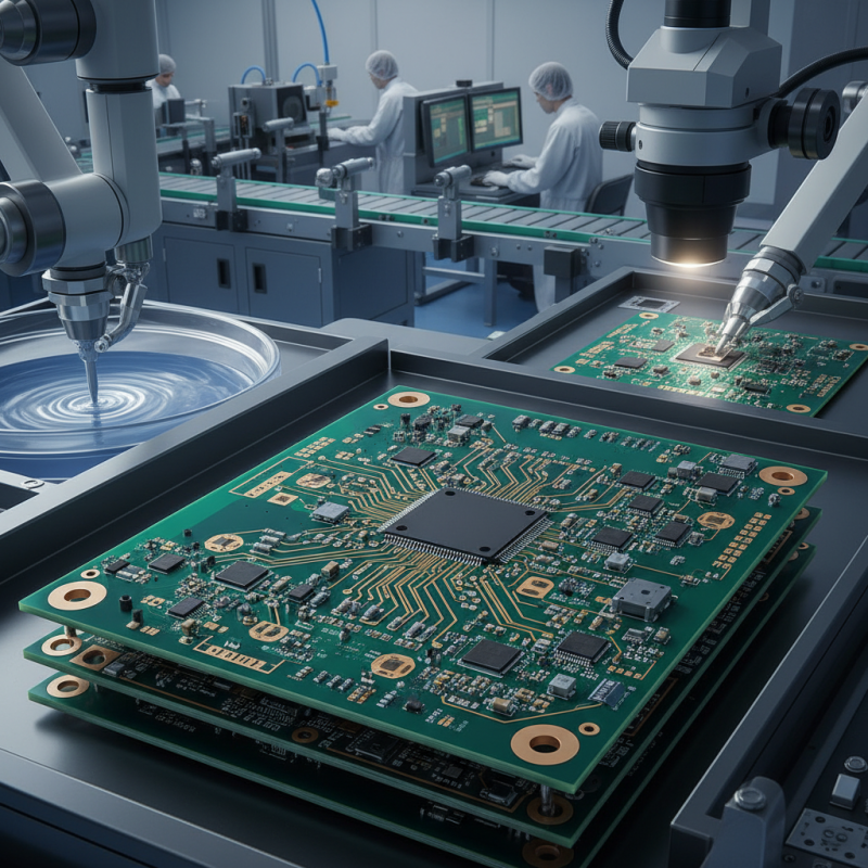
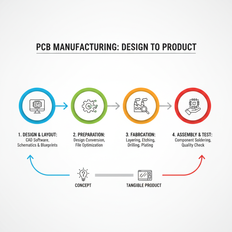
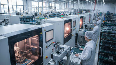
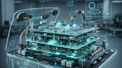
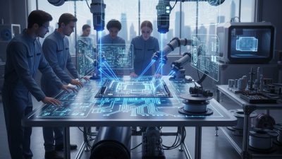
PCB fabrication is the intricate process of transforming design schematics into functional printed circuit boards (PCBs). This process begins with the creation of a digital layout, which employs software to define the circuitry, components, and pathways. Once the design is finalized, it is then transferred onto a substrate material, typically fiberglass-based, through various methods like photolithography. This technique uses light to etch the circuit pattern onto the board, allowing for precise placement of copper traces.
Following this, additional manufacturing steps are undertaken, including drilling holes for component placement and applying solder mask and silkscreen layers for protection and identification. Advanced fabrication technologies such as surface mount technology (SMT) streamline the assembly process, enabling components to be mounted directly onto the surface of the PCB. Other innovations include automated optical inspection systems that ensure quality control during production. Overall, understanding the PCB fabrication process provides insight into the foundational role that PCBs play in the electronics industry, impacting everything from consumer gadgets to complex industrial machinery.
This chart illustrates the various stages of the PCB fabrication process along with their respective time allocations. Understanding the distribution of time across different stages helps in analyzing the efficiency and optimization of PCB manufacturing.
PCB manufacturing is a meticulous process that transforms a conceptual design into a tangible product. The journey begins with the design phase, where engineers use software tools to create a detailed layout of the circuit board. This design includes specifications for the electrical connections, the placement of components, and the overall dimensions. Once finalized, the design is converted into a format suitable for production, ensuring that every detail is accurately represented for the next stages.
The subsequent step involves the preparation of the substrates, typically made of fiberglass or other insulating materials. These substrates are then coated with a thin layer of copper, which will later be etched away to form the desired circuit pathways. After etching, components are placed onto the board using automated machines, which precisely position and solder them into place. Finally, the assembled PCB undergoes rigorous testing to guarantee functionality and reliability. This careful, step-by-step approach ensures that the final product meets the required standards for performance and safety, paving the way for a successful integration into electronic devices.
The materials used in PCB (Printed Circuit Board) fabrication play a crucial role in determining the overall performance and reliability of the final product. Commonly utilized materials include FR-4, a widely used glass-reinforced epoxy laminate that provides excellent electrical insulation and mechanical strength. FR-4 is favored for its balance of performance and cost, making it suitable for a vast array of consumer electronics. However, for high-frequency applications, materials such as Rogers or Taconic, which offer lower dielectric loss and better thermal management, are often preferred to ensure signal integrity and reduce electromagnetic interference.
Another important aspect of PCB materials is the type of copper used for the conductive traces. The thickness and quality of copper can significantly affect the board's ability to handle power and heat dissipation. For high-power applications, thicker copper layers may be necessary to prevent overheating and ensure reliability over time. Additionally, surface finish options, including HASL, ENIG, and OSP, can influence solderability and corrosion resistance, further impacting the performance of the PCB in various environments. The careful selection of these materials is essential to meet specific application requirements and enhance the overall longevity and functionality of the PCB.
In the rapidly evolving field of PCB manufacturing, adherence to industry standards and rigorous quality control processes are paramount. According to a report by IPC, the global association for electronics manufacturing, approximately 60% of PCB defects stem from inadequate quality control measures during fabrication. This emphasizes the crucial role that standards such as IPC-A-600 (acceptability of printed boards) and IPC-6012 (qualification requirements for rigid PCBs) play in ensuring the integrity and reliability of PCBs used in various applications, from consumer electronics to aerospace.
Quality control in PCB manufacturing encompasses several key practices, including automated optical inspection (AOI) and X-ray inspection to detect hidden defects. A study by Research and Markets noted that the PCB inspection market is projected to grow by 5.34% annually, reflecting the increasing demand for high-quality electronic components. Implementing these standards and inspection techniques not only reduces costs associated with product failures but also enhances overall customer satisfaction by delivering reliable and efficient PCBs. As technology advances, the commitment to stringent industry standards will be vital for manufacturers aiming to maintain a competitive edge in the market.
| Dimension | Description | Standard Value | Unit |
|---|---|---|---|
| Copper Thickness | Thickness of copper layer on PCB | 1.0 | oz/ft² |
| Layer Count | Total number of layers in PCB | 4 | Layers |
| Minimum Trace Width | Narrowest width of a trace on PCB | 0.15 | mm |
| Minimum Distance Between Traces | Closest distance between two traces | 0.15 | mm |
| Drill Hole Size | Diameter of drilled holes for components | 0.3 | mm |
| Solder Mask Thickness | Thickness of the solder mask layer | 0.025 | mm |
| Finish Type | Type of surface finish applied | HASL | N/A |
Emerging trends in PCB fabrication are underscored by the increasing integration of automation and sustainable practices within the manufacturing ecosystem. Recent data indicates that the global market for industrial robots is projected to grow significantly, with an expected compound annual growth rate (CAGR) of approximately 10% from 2025 to 2035. This evolution is attributed to advancements in AI-driven technologies, which enhance precision and efficiency, ultimately streamlining production processes. The implementation of robotic automation in PCB manufacturing not only increases productivity but also helps in mitigating human errors, a crucial factor as the industry shifts towards smaller, more complex designs.
In parallel, sustainability is becoming a key focal point across electronic manufacturing services (EMS). With an increasing emphasis on reducing environmental impact, companies are adopting sustainable production methodologies and materials. For instance, the telecom EMS market is witnessing a transformation through the use of AI-powered machines that optimize the manufacturing of telecom devices while minimizing waste. Furthermore, new production technologies and techniques, such as single-use systems in biotech equipment, are reshaping traditional manufacturing lines, emphasizing the importance of innovation in a competitive landscape. The shift towards automation and sustainability not only enhances operational efficiency but also aligns with global initiatives for greener manufacturing practices, catering to the rising consumer demand for environmentally friendly products.