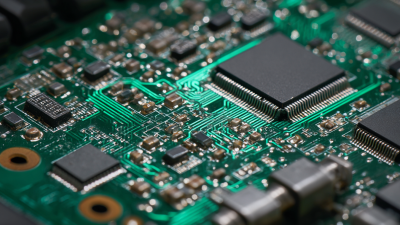
In the rapidly evolving landscape of electronics, the efficiency of product development hinges significantly on effective PCB prototyping strategies. As we look towards 2025, industry experts recognize the importance of integrating digital innovations in PCB prototyping to streamline the development process.
Paul K. Johnson, a renowned expert in PCB design, emphasizes, "The future of electronics is rooted in how seamlessly we can prototype our PCBs, enabling faster iterations and promoting innovation."
The integration of advanced digital tools not only enhances the accuracy of prototypes but also facilitates collaboration among teams, ultimately leading to faster time-to-market. By leveraging "digital + best practices" in PCB prototyping, companies can achieve a competitive edge, ensuring that their products meet market demands swiftly and effectively. This approach supports a holistic view of product development, where each prototype serves as a critical stepping stone towards a final product that exceeds customer expectations and industry standards.
As we delve into 2025 strategies for PCB prototyping, it is crucial to understand the transformative impact of these practices on product development efficiency. By harnessing the power of technology and expert insights, businesses can navigate the complexities of modern electronics, paving the way for innovative solutions that resonate in a fast-paced market.
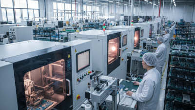
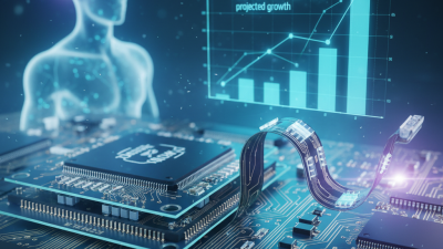
In the rapidly evolving landscape of PCB prototyping, integrating AI-driven design tools is proving to be a game-changer for product development efficiency. According to a recent industry report by IPC, companies implementing AI technologies in their design processes can reduce prototyping time by up to 30%. This efficiency gain not only accelerates time-to-market but also enhances design accuracy, minimizing costly errors that can occur during manual processes. By leveraging algorithms that predict design flaws and suggest optimizations, engineers can focus more on innovation rather than troubleshooting.
Tips: Consider adopting AI tools that offer design validation features. These can analyze your design against manufacturing capabilities early in the process, significantly reducing iterations and unnecessary modifications.
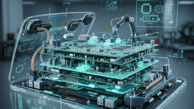
Moreover, the use of AI in PCB prototyping enables simulation and testing of designs in virtual environments before actual production. A study published in the Journal of PCB Design shows that teams utilizing AI simulation tools see a 25% decrease in material costs due to optimized resource allocation. As businesses increasingly recognize the value of these innovations, it's essential to stay ahead by continually updating your design processes with the latest AI advancements.
Tips: Invest in training for your design team on AI tools and software to fully utilize their capabilities. This will enhance their skill set and ensure a smoother transition to these advanced technologies.
The integration of advanced simulation software in PCB prototyping is revolutionizing product development efficiency. As companies increasingly embrace AI-powered design tools, they are witnessing substantial improvements in design verification processes. Recent strategic partnerships within the semiconductor domain have highlighted the growing importance of these technologies. For instance, a noteworthy collaboration has emerged in which leading firms are leveraging AI-enhanced design tools to achieve significant outcomes, including increasing the first silicon success rate.
According to industry reports, nearly 70% of engineering teams utilizing advanced simulation software have reported reduced prototype development timelines. Additionally, the ability to conduct comprehensive design validation in virtual environments has minimized the need for costly physical modifications, empowering teams to iterate designs quickly. This shift towards simulation-driven methodologies not only accelerates the R&D cycle but also leads to more reliable end products, ultimately benefiting overall business performance. By investing in cutting-edge verification tools, companies can harness optimal design accuracy and efficiency, paving the way for innovation in PCB prototyping.
The integration of IoT technologies into PCB testing processes is revolutionizing the way companies approach product development. According to a recent industry report by ResearchAndMarkets, the global IoT in electronics market is projected to reach $8.5 billion by 2025, highlighting the growing importance of interconnected devices in streamlining operations. By utilizing IoT sensors and devices during the testing phase, manufacturers can gather real-time data on performance and functionality, minimizing the risks of defects in the final products.
Moreover, the adoption of smart testing solutions enables instant feedback loops, which significantly enhance the efficiency of PCB prototyping. A study from Gartner indicates that organizations implementing IoT-driven testing methods can reduce their time-to-market by up to 30%. This acceleration in product development not only allows for quicker iterations and refinements based on immediate insights but also fosters innovation as designers can experiment more freely without the constraints of lengthy testing cycles. By removing traditional bottlenecks through smart technology, companies can stay competitive in a rapidly evolving market.
The integration of agile methodologies into PCB prototyping signifies a paradigm shift in product development efficiency. By adopting iterative processes, teams can enhance communication, adapt quickly to changes, and improve overall workflow. Agile principles such as collaboration, flexibility, and continuous feedback allow engineers to respond promptly to design alterations, minimizing the time and cost associated with traditional prototyping methods. This approach encourages regular review cycles, ensuring that each iteration meets evolving project requirements and stakeholder expectations.
Furthermore, implementing agile practices fosters a culture of innovation within teams. By breaking down the prototyping process into smaller, manageable tasks, team members can focus on specific components, accelerating the identification of potential issues early on. Frequent testing and validation not only lead to higher product quality but also reduce the risk of costly revisions at later stages of development. With timely adjustments and constant iteration, agile methodologies empower organizations to bring PCB prototypes to market faster, ultimately enhancing their competitive edge in an increasingly dynamic industry landscape.
| Strategy | Description | Expected Outcome | Implementation Timeline |
|---|---|---|---|
| Rapid Prototyping Techniques | Utilizing 3D printing and CNC machining for quick PCB prototypes. | Decreased prototype lead time by up to 50%. | Q1 2025 |
| Agile Development Framework | Implementing iterative design and development cycles. | Improved team collaboration and faster feedback loops. | Q2 2025 |
| Collaboration Tools | Adopting digital tools for real-time communication between teams. | Enhanced clarity and reduced errors in design specifications. | Q1 2025 |
| Customer Feedback Integration | Incorporating user feedback in early prototyping stages. | Higher satisfaction rates and product market fit. | Ongoing throughout 2025 |
| Cross-functional Teams | Creating teams with diverse expertise for holistic design reviews. | Improved innovation and reduced project bottlenecks. | Q3 2025 |
In 2025, the strategies for PCB prototyping will play a critical role in enhancing product development efficiency, particularly through a focus on cost-benefit metrics. By leveraging advanced technologies and methodologies, organizations can minimize costs while maximizing the output quality of prototypes. This is especially relevant in industries such as agriculture, where the introduction of tailored solutions—like custom-built agri-drones—has already demonstrated significant time savings during field trials. The 70% reduction in manual monitoring time showcases the advantages of integrating innovative technologies, which can similarly be applied to PCB prototyping.
Additionally, the move towards sustainable electronics and streamlined manufacturing processes will further bolster efficiency metrics in PCB design. As companies increasingly turn to data-driven practices, the ability to detect surface defects through automated systems can lead to significant reductions in production time and costs. This evolution emphasizes the importance of adopting robust electronic design automation tools and AI-driven optimization strategies, ensuring that the projects not only remain economically viable but also environmentally responsible. By focusing on these cost-benefit metrics, companies can navigate the complexities of product development in 2025, driving innovation while maintaining competitive advantages.