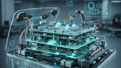
What is Printed PCB and How Does It Work?
Printed PCBs, or printed circuit boards, are integral to modern electronics. They serve as the backbone for countless devices, from smartphones to medical equipment. Dr. Emily Tran, a leading expert in electronics manufacturing, notes, “Understanding printed PCBs is crucial for innovation in technology.” Her perspective underscores the importance of this technology in shaping our digital world.
Printed PCBs consist of conductive tracks and pads. These components connect various electronic parts, allowing them to communicate. Their reliable performance is essential for the efficiency of any device. However, the complexity of designing printed PCBs can lead to production challenges. Mistakes in layout or material choice can have lasting impacts on functionality.
As industries advance, the demand for high-quality printed PCBs grows. This evolution pushes manufacturers to innovate. They must balance quality and cost without compromising effectiveness. However, overlooking the fundamentals of printed PCB design can hinder progress. So, understanding this technology is vital for anyone involved in electronics today.
What is a Printed Circuit Board (PCB)?
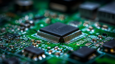
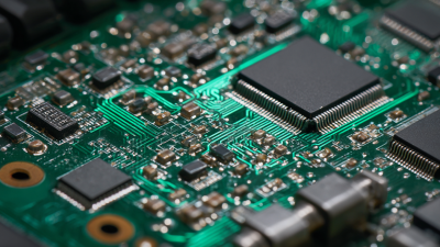
A Printed Circuit Board (PCB) is a crucial component in modern electronics. It serves as a foundation for connecting various electronic parts. This board is typically made from materials like fiberglass or a similar substance that provides insulation and structural support. The conductive paths on the PCB are created using copper traces, meticulously designed to ensure efficient signal flow.
PCBs come in various shapes and sizes, depending on their application. Some circuits are simple, while others are complex, featuring multiple layers. Designing a PCB requires careful consideration and attention to detail. Mistakes, like incorrect trace width, can lead to malfunction. It’s a precise balancing act between functionality and manufacturability.
One of the challenges in PCB design is managing heat dissipation. Components generate heat, and excessive heat can lead to failures. Proper layout and materials selection are essential to prevent overheating. It’s an area that often needs improvement for better performance. Learning from past designs can lead to better future products.
History and Evolution of Printed PCBs
The history of printed circuit boards (PCBs) dates back to the early 20th century. The concept of interconnecting electronic components began in the 1920s. However, it was not until the 1940s that the first true printed circuit boards were developed. This innovation significantly transformed the electronics industry.
By the 1950s, the demand for more compact and efficient electronics surged. Manufacturers needed a solution to handle the increasing complexity of circuits. This led to advancements in PCB technology. Layering techniques allowed for multiple circuits on a single board. These developments made devices smaller and more efficient.
Despite these advancements, challenges remain. Modern PCBs must meet increasing performance demands while remaining cost-effective. The rush for innovation can sometimes overlook crucial aspects like environmental impact and product longevity. As technology evolves, there is a continuous need for reflection and improvement. Balancing innovation with responsibility is crucial for the future of PCBs.
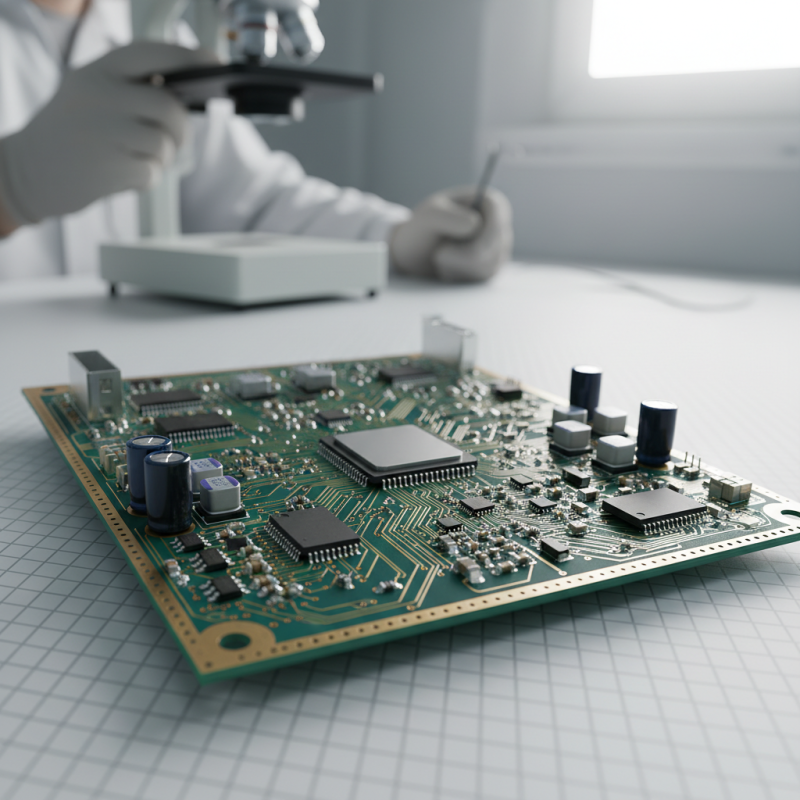
Components and Materials Used in PCB Manufacturing
Printed circuit boards (PCBs) are essential in modern electronics. The manufacturing process involves various components and materials that influence performance and reliability. Copper is a primary conductor used, often in thin layers. According to industry reports, approximately 30% of PCB failures result from poor copper quality or inconsistencies.
The substrate material also plays a critical role. FR-4, a glass-reinforced epoxy laminate, is widely used due to its balance of cost and electrical properties. However, not all FR-4 materials are produced equally. Variations in manufacturing can lead to weaknesses in thermal performance. This inconsistency can pose risks in high-temperature applications.
Moreover, solder mask and silkscreen layers are vital for protecting and marking. The solder mask prevents solder bridging and helps in preventing corrosion. Reports suggest that improper application can lead to significant failure rates in finished products. Thus, every step in the PCB manufacturing process needs careful consideration to meet industry standards and ensure longevity.
Components and Materials Used in PCB Manufacturing
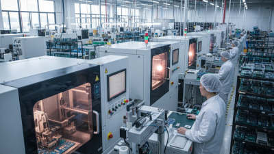
How PCBs are Fabricated and Assembled
When it comes to printed circuit boards (PCBs), understanding their fabrication and assembly is crucial. The process starts with designing the PCB layout using specialized software.
This layout includes the placement of components and the routing of electrical connections. Designers must ensure that the traces do not short circuit, which can be a common error.
Once the design is complete, the next step is fabrication. This involves etching copper onto a substrate material, such as fiberglass. The result is a board with conductive pathways. An error here can lead to incomplete circuits. It's important to maintain precision throughout the process.
After fabrication, the assembly phase begins. Components like resistors and capacitors are soldered onto the PCB. Automated machines often perform this task. However, human oversight is still needed to catch mistakes, such as misplaced components.
Quality control is essential, as a single faulty connection can disrupt the entire function of a PCB. The entire process requires careful attention to detail, and even minor oversights can lead to major complications.
Functionality and Applications of Printed PCBs
Printed PCBs, or printed circuit boards, are essential in modern electronics. They serve as the backbone for nearly all electronic devices. Their functionality stems from their ability to connect various electronic components through conductive pathways. These pathways are etched onto a non-conductive substrate. The connections allow current to flow, enabling components to communicate and perform their designated tasks.
Applications of printed PCBs are vast and diverse. They are found in everyday items like smartphones, computers, and appliances. In automotive technology, PCBs are crucial for functions such as engine control and navigation systems. The medical field also benefits from printed PCBs in devices like monitors and diagnostic instruments. However, there's room for improvement. As technology evolves, PCBs need to adapt to more compact designs and higher frequencies. Innovations in materials and manufacturing processes could enhance performance but raise production costs and environmental concerns.
Some challenges persist in PCB production. Issues like signal interference and thermal management must be addressed. Designing for durability and reliability is complex. Engineers must navigate these issues while balancing cost and functionality. Continuous refinement is necessary to keep pace with advancements in technology. This ongoing journey highlights the need for innovation in PCB design and production.