Efficient and cost-effective PCB prototyping can transform design processes significantly. In today's fast-paced market, having a reliable prototyping method is crucial. Designers often face various challenges like high costs and lengthy production times. This demands innovative solutions that can streamline the workflow while minimizing expenses.
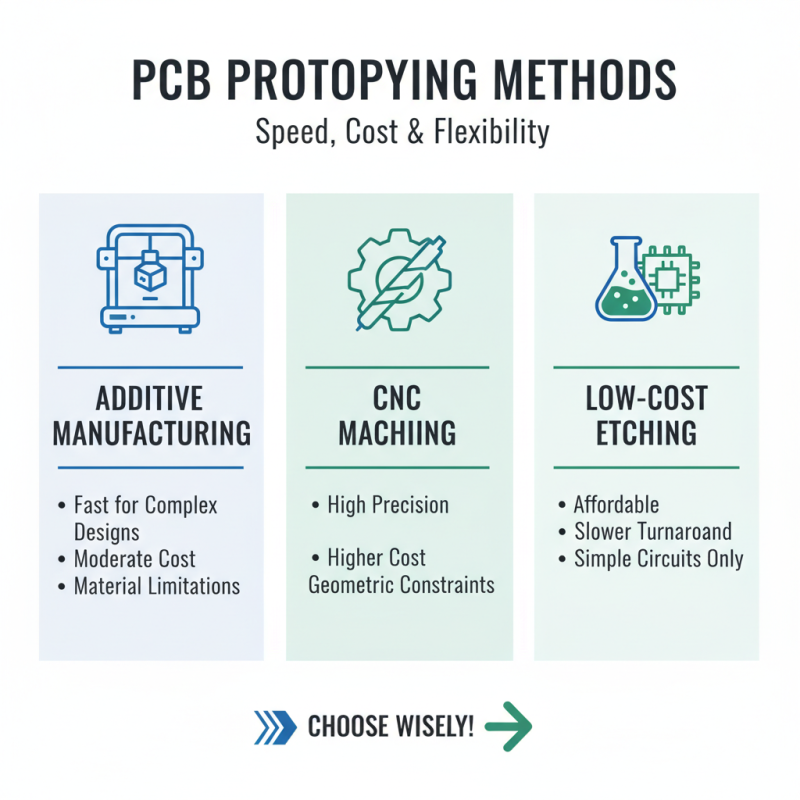
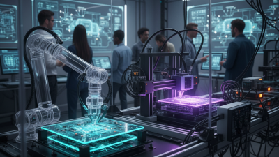
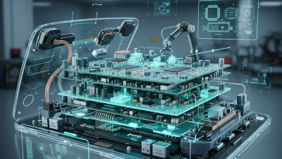
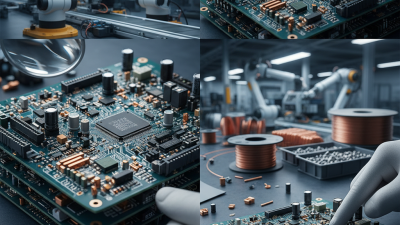
PCB prototyping techniques have evolved to meet these needs. Techniques such as rapid prototyping and 3D printing offer quick iterations. These methods allow engineers to test their designs before full-scale production. However, not all techniques guarantee perfect results. Issues like material selection and manufacturing precision can lead to setbacks. Engineers must evaluate their needs carefully.
Additionally, choosing the right prototyping technique depends on the project scale and budget. Some methods may seem efficient but could escalate costs unexpectedly. A thorough understanding of each technique aids in making informed decisions. Exploring these techniques can pave the way for optimal designs that align with both creativity and practicality.
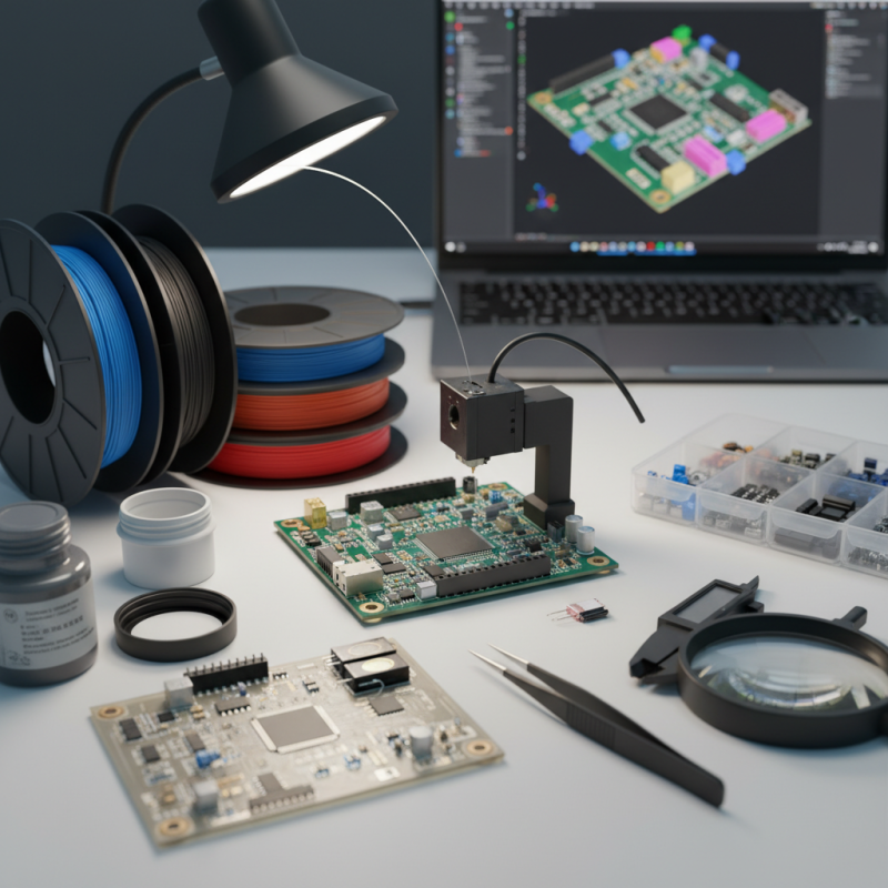
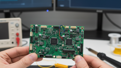
PCB prototyping is essential for effective design. It allows engineers to test ideas quickly. Rapid iterations help spot flaws early. Creating prototypes fosters innovation.
One principle is to minimize complexity. A simple design is easier to prototype. Complex layouts can lead to more errors. When starting, focus on essential functions. This will save time and resources.
Testing should be thorough. Every prototype must undergo scrutiny. Some may not meet expectations. This is a chance for reflection and improvement. Feedback loops are crucial. Adjust and refine designs based on testing results. Embrace the imperfections of the process. They lead to better outcomes.
When it comes to PCB prototyping, various techniques can enhance cost efficiency. One common method is using breadboards. Breadboards allow rapid testing without soldering. This can save time and reduce material costs. However, they do have limitations in terms of complexity. If the design becomes too intricate, breadboards can become impractical.
Another technique involves using 3D printing for components. This approach is innovative and allows for quick adjustments. Designers can create custom shapes on-the-fly. It’s less traditional but increasingly popular. Yet, the quality of printed parts may sometimes lead to unexpected failures in circuits. This is an area that needs careful evaluation.
**Tips:** Always evaluate your design complexity against your prototyping method. Don't overlook the material quality. Conduct tests frequently and learn from any failures. Experimentation is essential in PCB design. Reach out to peers for feedback on your prototypes. Their insights can lead you to refine your designs further.
In the world of PCB prototyping, selecting the right method can be crucial. Rapid prototyping plays a significant role in quickly bringing ideas to life. Techniques such as additive manufacturing, CNC machining, and low-cost PCB etching have their strengths and weaknesses. Each method has distinct characteristics that impact cost, speed, and design flexibility.
Additive manufacturing is gaining traction due to its ability to produce complex geometries. It allows for detailed designs that would be challenging with traditional methods. However, layer adhesion issues can arise, leading to structural weaknesses in some cases. CNC machining offers precision but typically requires more time and resources. The setup for CNC processes can be costly, which may not be ideal for early-stage prototyping.
Low-cost PCB etching provides a budget-friendly option. This method is suitable for simpler designs and can be completed in-house. However, it often lacks the precision of other methods and can lead to inconsistent results. Designers need to carefully weigh these pros and cons before deciding on a technique. Each method invites reflection on how effectively it meets the project's unique demands.
In PCB prototyping, minimizing errors is crucial for an efficient design. One common mistake is ignoring the importance of a thorough design review. A second set of eyes can catch issues that one might overlook. Schedule regular reviews during the prototyping phase to identify potential problems early on. This simple step can save time and resources later.
Testing and validation are also vital. Rushing through the testing process often leads to failure in the final product. Conducting multiple test iterations can reveal design flaws before mass production. Additionally, using simulation software helps visualize potential issues. Yet, relying entirely on simulations can be misleading. Always cross-check results with physical prototypes.
Documentation plays a critical role in minimizing errors as well. Clear and concise documentation ensures that everyone involved understands the design intent. However, teams sometimes skip thorough documentation, leading to confusion. Encourage your team to maintain detailed notes throughout the process. This practice promotes better communication and can prevent costly mistakes. Attention to detail in these areas can significantly enhance the overall quality of PCB prototypes.
When designing printed circuit boards (PCBs), material choice is crucial for cost-effectiveness. Materials significantly impact the overall production cost and performance of PCBs. Research shows that the selection of materials can account for up to 30% of the total project budget. This means that engineers must carefully assess different substrates, copper weights, and thicknesses before committing to a design.
For instance, FR-4 is a popular choice due to its balance of cost and performance. It offers decent thermal and electrical properties at a low price. However, there are trade-offs. While FR-4 serves many applications, specific high-frequency applications may require alternative materials, leading to increased costs. This highlights the importance of evaluating the desired performance versus the material cost.
Additionally, design complexity can elevate manufacturing costs. Poor choice of materials or excessively intricate designs might result in unforeseen expenses. Feedback from industry reports indicates that optimizing the PCB layout can save up to 20% in manufacturing costs. Proper design techniques and material evaluation can lead to both cost savings and efficiency improvements in PCB prototypes. Thus, engineers should scrutinize their material choices to strike a balance between quality and affordability.
| Technique | Material Type | Cost ($/sq ft) | Lead Time (Days) | Common Applications |
|---|---|---|---|---|
| Laser Cutting | FR-4 | 5.00 | 7 | Consumer Electronics |
| 3D Printing | PLA | 3.00 | 5 | Prototyping |
| CNC Milling | Aluminum | 10.00 | 14 | Industrial Equipment |
| Chemical Etching | Copper | 4.50 | 10 | Electronics |
| Thermal Transfer Printing | Polyimide | 7.50 | 3 | Flexible Circuits |