Top 10 Tips for Efficient PCB Creation: Boost Your Design Skills Today!
In the ever-evolving world of electronics, the ability to efficiently create printed circuit boards (PCBs) is crucial for engineers and designers alike. According to Dr. Emily Carter, a leading expert in PCB design and a professor at the Institute of Electronics Engineering, "Mastering the art of PCB creation is not just about technical skills; it’s about understanding the intricate balance between design functionality and manufacturability." This insight emphasizes the importance of not only technical proficiency but also the strategic thought that goes into effective PCB creation.
As the demand for innovative electronic devices grows, so does the need for optimized PCB design processes. Understanding the best practices and tools available can significantly enhance a designer’s capability to deliver high-quality PCBs efficiently. In this article, we will explore the top ten tips for efficient PCB creation, offering insights that can help you sharpen your design skills and improve your workflow. Whether you are a seasoned professional or a newcomer to the field, these strategies will aid in navigating the complexities of PCB design, ensuring your projects not only meet specifications but also excel in performance and reliability.

Understanding the Basics of PCB Design for Beginners
Understanding the basics of PCB design is crucial for beginners looking to make their mark in the electronics industry. According to a report by Research and Markets, the global PCB market is projected to grow to $75 billion by 2025, driven by advancements in technology and the increasing demand for consumer electronics. With the rise of smart devices and IoT applications, mastering PCB design has never been more essential for aspiring engineers.
Beginners should start by familiarizing themselves with fundamental concepts such as schematic capture, layout design, and signal integrity. The IPC standards, which govern PCB manufacturing and assembly, provide a valuable framework for ensuring quality and reliability in designs. A solid understanding of software tools utilized in PCB design, like CAD systems, can enhance efficiency and accuracy. In fact, a survey conducted by the Institute for Printed Circuits suggests that 70% of successful PCB designers attribute their achievements to a comprehensive understanding of these software tools and the design process. By gaining proficiency in these areas, newcomers can significantly elevate their design skills and contribute effectively to their projects.
Essential Software Tools for Streamlined PCB Creation
In today's fast-paced electronics landscape, the effective creation of printed circuit boards (PCBs) hinges significantly on the selection of the right software tools. According to a recent industry report by the IPC (Institute of Printed Circuits), over 60% of engineering teams cite inadequate tools as a primary barrier to efficient PCB design. To address this challenge, leveraging advanced software solutions can streamline processes, enhance collaboration, and ultimately improve design outcomes.
Essential tools for PCB creation often include schematic capture, layout software, and simulation tools. Schematic capture programs allow designers to create and modify circuit diagrams efficiently, while layout software translates these diagrams into physical PCB designs. The integration of simulation tools is increasingly crucial, as it enables engineers to foresee potential issues and enhance functionality before production. A survey by TechValidate revealed that 75% of firms that adopted comprehensive PCB design software reported a significant reduction in prototyping time, underscoring the importance of employing robust tools in the design cycle.
Moreover, many modern PCB design software solutions incorporate cloud connectivity, facilitating real-time collaboration among team members located in different geographical regions. This capability is especially beneficial as the demand for remote work continues to rise. In fact, a study by Deloitte indicated that organizations embracing cloud-based design tools noticed a 30% increase in overall project efficiency. Emphasizing the right combination of software tools is crucial in cultivating efficient PCB creation practices that not only save time but also enhance the overall quality of electronic products.
Top 10 Tips for Efficient PCB Creation: Boost Your Design Skills Today!
| Tip No. |
Tip |
Description |
Essential Software Tool |
| 1 |
Start with a Good Design |
Plan your layout and specifications carefully to avoid rework. |
Altium Designer |
| 2 |
Use Standard Components |
Selecting common components can simplify sourcing and assembly. |
KiCad |
| 3 |
Optimize Your Layout |
Arrange components for minimal trace lengths to enhance performance. |
Eagle |
| 4 |
Conduct Design Rule Checks |
Use DRC tools to catch errors before manufacturing. |
OrCAD |
| 5 |
Incorporate Thermal Management |
Design with heat dissipation in mind to improve device reliability. |
Fusion 360 |
| 6 |
Keep Trace Widths Consistent |
Use uniform trace widths to maintain signal integrity and manufacturing ease. |
PADS |
| 7 |
Plan for Testing |
Ensure easy access to test points in your design for quicker diagnostics. |
Altium Designer |
| 8 |
Document Your Design |
Maintain comprehensive documentation for future reference and updates. |
Microsoft Office |
| 9 |
Review and Revise Regularly |
Schedule regular reviews to continually improve your design skills. |
Trello |
| 10 |
Get Feedback |
Collaborate with peers to gain insights and improve your designs. |
Slack |
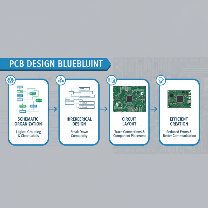
Best Practices for Schematic Design and Circuit Layout
When embarking on the journey of PCB design, understanding best practices for schematic design and circuit layout is crucial to facilitate efficient and effective creations. A well-structured schematic acts as the blueprint for your PCB, enabling better communication of ideas and preventing errors in the later stages of design. Start by organizing your components logically; group related items together to enhance readability. Labeling components clearly and utilizing consistent symbols can significantly reduce confusion, making it easier to track connections during circuit layout. Additionally, make use of hierarchical design, allowing for complex systems to be broken down into manageable sections.
Circuit layout further emphasizes the importance of clarity and precision. Maintaining a proper spacing between traces, using ground planes wisely, and ensuring adequate trace width will minimize interference and enhance the reliability of the final product. Employ design rules checks regularly throughout the layout process to identify potential design flaws early. Furthermore, consider the physical placement of components based on signal flow and thermal management. An efficient layout not only improves performance but also simplifies manufacturing and assembly, ensuring that your PCB functions optimally in its intended application. By adhering to these best practices in schematic design and circuit layout, designers can drastically enhance their PCB development process.
Tips for Optimizing PCB Manufacturing Processes
When optimizing PCB manufacturing processes, several key factors can significantly enhance efficiency and reduce costs. According to a report by IPC, nearly 70% of PCB manufacturing defects are associated with design errors. This statistic underscores the importance of effective design practices right from the outset. Implementing design-for-manufacture (DFM) principles can help ensure that PCB designs are not only optimal for functionality but also for manufacturability. For instance, keeping trace widths consistent and minimizing the number of layers can lead to significant reductions in production time and material waste.
Moreover, adopting modern manufacturing technologies, such as automated optical inspection (AOI) and advanced surface mount technology (SMT), can dramatically improve process efficiency. Research from the Electronics Industry Association indicates that the integration of automation in PCB assembly lines can decrease the average manufacturing cycle time by as much as 30%. By utilizing these technologies, manufacturers are able to catch defects earlier in the process, which reduces costly reworks and helps maintain quality standards. Investing in training for engineers on the latest tools and software is another crucial step, as skilled personnel can leverage advanced simulation tools to predict potential manufacturing issues before they occur. This proactive approach not only saves time but also fosters innovation, leading to high-quality, reliable PCB products.
Top 10 Tips for Efficient PCB Creation
Testing and Validation Techniques for PCB Designs
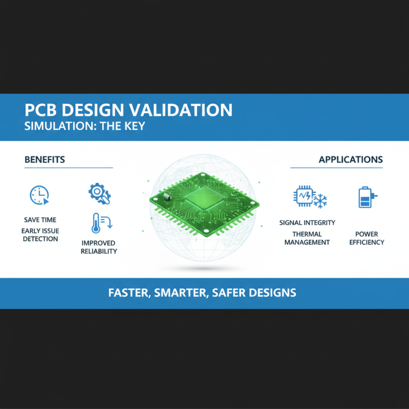
Testing and validation are crucial components of the PCB design process, as they ensure that the final product meets performance and reliability standards. One effective approach to validate PCB designs is through simulation. Using specialized software, designers can create virtual prototypes of their circuits, allowing them to assess performance under various conditions without the need for physical prototypes. This not only saves time but also helps identify potential issues early in the design phase, such as signal integrity problems or thermal management challenges.
Another essential technique is the use of prototype testing after the initial design is completed. By fabricating a small run of the PCB and conducting real-world tests, designers can gather valuable data on the functionality and durability of their designs. This hands-on approach can unveil issues that simulations might overlook, such as unexpected electromagnetic interference or layout problems. Furthermore, incorporating tools like Automated Optical Inspection (AOI) and Functional Testing can ensure that the manufactured PCBs adhere to the intended design specifications, significantly reducing the risk of failure in end-use applications.