
What Is Rigid Flex PCB and How Does It Work?
A rigid flex PCB combines rigid board sections with flexible circuit layers in one engineered assembly. It can bend. It can also support components. This hybrid structure reduces connectors, cables, and assembly space inside compact electronics. Imagine a camera module folding around a battery without a loose wire harness. The result is cleaner routing and fewer mechanical connection points.
The rigid areas usually contain reinforced dielectric layers, copper traces, and component footprints. Flexible sections use thin polyimide films, copper, and carefully designed coverlay protection. During operation, signals travel continuously through copper paths across rigid and flexible zones. The flexible portion bends within a defined radius, while rigid portions hold chips, sensors, or connectors securely. A well-designed stackup controls impedance, heat, and mechanical stress. Manufacturing quality matters greatly here. Small alignment errors can weaken reliability.
This article explains what rigid flex technology is and how it works in real products. It examines layer construction, bending behavior, signal transmission, fabrication, testing, and common design decisions. Experienced engineers know that flexibility does not mean unlimited movement. Repeated folding, sharp corners, excessive copper, or poor support can cause cracks over time. That limitation is easy to overlook. Design rules also vary by material, supplier, and application. Reliable results require documented specifications, prototype testing, and inspection against accepted industry practices. The technology is powerful, but not automatically better. Its value depends on whether mechanical and electrical requirements truly justify the added design complexity.
What Is a Rigid-Flex PCB?
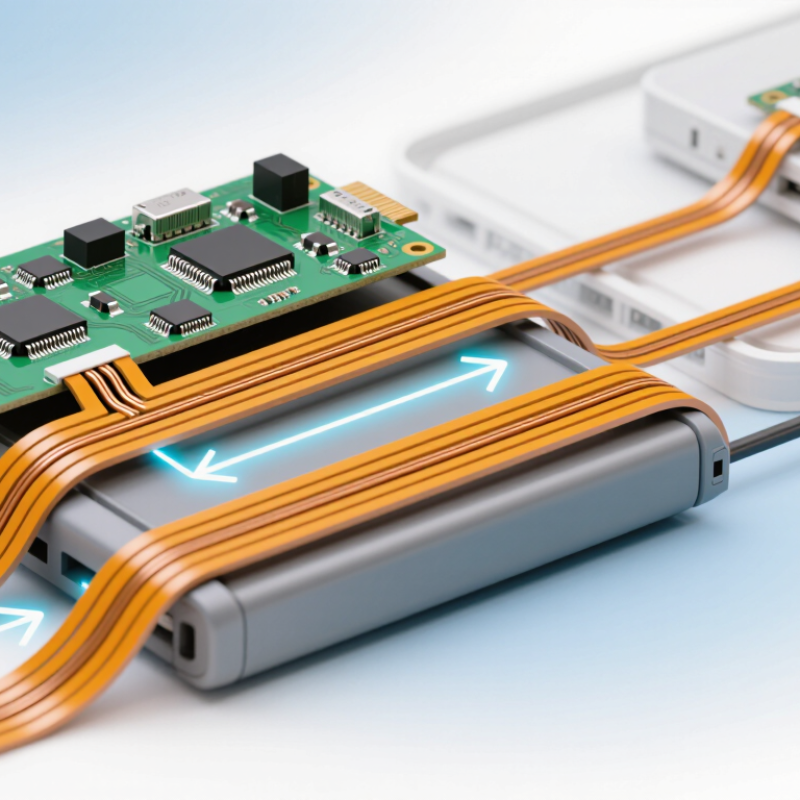
A rigid-flex PCB combines rigid board sections with flexible polyimide layers. It is not simply a rigid PCB with a bendable cable attached. The layers are laminated into one interconnected structure. Copper traces travel through both rigid and flexible zones, while plated vias carry signals between layers. This design can replace connectors, cables, and extra assembly points inside compact equipment.
The engineering value is clear. A 2024 MarketsandMarkets estimate places the rigid-flex PCB market near USD 3.5 billion, with growth toward approximately USD 5.8 billion by 2029. However, market estimates vary by research method. Designers must still verify bend radius, copper thickness, layer stack-up, and thermal limits. IPC-2223 provides design guidance for flexible and rigid-flex circuits. In practice, repeated bending can damage copper if the bend area is poorly supported. Small layout decisions matter.
Tips: Keep components away from dynamic bend zones. Use gradual transitions between rigid and flexible sections. Confirm the minimum bend radius with the fabricator. Add strain relief near connectors and stiffeners. Prototype early. A design may pass electrical tests but fail after mechanical cycling. That uncomfortable gap deserves attention.
What Is Rigid Flex PCB and How Does It Work? - What Is a Rigid-Flex PCB?
| Data Dimension | Typical Information | How It Relates to Rigid-Flex PCB Design and Operation |
|---|---|---|
| Basic Definition | A rigid-flex PCB combines rigid circuit-board sections with one or more flexible circuit sections in a single interconnected assembly. | The rigid areas provide mechanical support and component-mounting surfaces, while the flexible areas allow the circuit to bend, fold, or move during installation and operation. |
| Primary Construction | Typical structures include rigid laminate layers, flexible polyimide layers, copper conductors, coverlay, solder mask, plated-through holes, and stiffeners. | These materials are laminated and interconnected so that electrical signals can pass continuously between rigid and flexible portions without requiring separate cable assemblies or board-to-board connectors. |
| Rigid Section | Common rigid sections use glass-reinforced epoxy laminate or other rigid dielectric materials. | Rigid sections are used where the design needs dimensional stability, connector support, heat spreading, or a firm platform for surface-mounted components. |
| Flexible Section | Flexible sections commonly use polyimide-based dielectric films with rolled or electrodeposited copper conductors. | The flexible region is designed to withstand controlled bending. Its bend radius, copper type, layer count, and bend direction must be considered during layout and mechanical integration. |
| Electrical Operating Principle | Conductive copper traces carry power and signals through both rigid and flexible regions. | The circuit functions like a conventional multilayer PCB electrically, but the interconnect path can change shape mechanically without interrupting the designed electrical connection. |
| Typical Layer Configuration | Configurations may be single-sided, double-sided, or multilayer, with rigid and flexible layer counts selected for the application. | More layers can support higher routing density and controlled impedance, but they generally increase thickness, stiffness, manufacturing complexity, and cost. |
| Dynamic vs. Static Flexing | Static flexing means the circuit is bent during assembly and then remains substantially stationary. Dynamic flexing means it bends repeatedly during operation. | A design intended for repeated movement requires stricter control of bend radius, copper geometry, neutral-axis placement, materials, and flex-cycle testing than a design that is bent only once. |
| Bend Radius | The minimum bend radius depends on factors such as total flex thickness, copper type, layer count, and whether the bend is static or dynamic. | Using a bend radius that is too small can create copper fatigue, cracking, delamination, or changes in electrical performance. The manufacturer’s material-specific design rules should be followed. |
| Electrical Interconnection | Rigid and flexible sections may be connected through plated vias, buried or blind structures where applicable, and continuous copper patterns. | Integrated interconnections can reduce the number of detachable interfaces, which may improve packaging efficiency and reduce assembly-related connection points. |
| Component Mounting | Components are normally mounted on rigid areas; selected components may also be mounted on properly supported flexible areas. | Keeping heavier or mechanically stressed components on rigid sections helps limit flex-region strain and supports more reliable solder joints. |
| Space and Packaging Efficiency | Rigid-flex boards can be folded into three-dimensional assemblies and routed through constrained spaces. | This can reduce the space occupied by separate PCBs, wires, connectors, and cable-routing hardware in compact electronic products. |
| Weight Reduction | Replacing multiple boards and cable assemblies with one integrated rigid-flex structure can reduce overall interconnect hardware. | Weight reduction is especially useful in portable, handheld, aerospace, medical, and other applications where packaging volume and mass are limited. |
| Signal Integrity | Controlled-impedance traces, suitable stackups, short interconnect paths, and careful flex-region routing can support high-speed signaling. | Signal performance can be affected by changes in geometry, dielectric thickness, bend configuration, vias, and transitions between rigid and flexible regions. |
| Thermal Considerations | Rigid sections generally provide more options for component support and thermal management than thin flexible sections. | Heat-generating components are commonly placed on rigid areas, while flexible areas are kept away from excessive heat and sharp thermal gradients where possible. |
| Reliability Benefits | An integrated design can eliminate some wire harnesses, plug-in connectors, and manual cable assemblies. | Fewer detachable interfaces can reduce risks associated with connector wear, assembly variation, vibration, and accidental disconnection. |
| Key Reliability Risks | Common risks include copper fatigue, flex cracking, delamination, solder-joint stress, adhesive failure, and damage caused by over-bending. | Reliability depends on correct mechanical constraints, adequate bend relief, appropriate materials, controlled lamination, and validation under expected temperature, vibration, and flex-cycle conditions. |
| Manufacturing Process | Typical steps include material preparation, circuit imaging, etching, drilling, plating, lamination, coverlay or solder-mask application, surface finishing, routing, inspection, and testing. | Rigid-flex fabrication requires alignment and process control across materials with different thickness, stiffness, thermal expansion, and handling characteristics. |
| Design Constraints | Important constraints include bend radius, flex-zone boundaries, copper spacing, via placement, stiffener location, component clearance, and allowable mechanical strain. | Components, vias, and sharp copper features are generally kept away from the active bend area unless the design has been specifically engineered and qualified for that condition. |
| Common Applications | Examples include compact consumer electronics, cameras, automotive modules, industrial controls, medical equipment, aerospace electronics, and instrumentation. | These applications benefit when electronic assemblies must fit irregular spaces, tolerate movement, reduce wiring, or combine multiple circuit sections into a compact package. |
| Main Advantages | Compact three-dimensional packaging, reduced connector count, lower wiring complexity, improved assembly integration, and potential weight savings. | These advantages can improve product packaging and assembly efficiency when the rigid-flex design is optimized for the required electrical, mechanical, thermal, and environmental conditions. |
| Main Limitations | Rigid-flex boards generally require more specialized materials, design rules, fabrication steps, inspection, and testing than standard rigid PCBs. | Higher initial cost and longer design qualification may be justified when the application requires flexibility, space savings, improved integration, or reduced connector-related risk. |
| Recommended Validation | Validation may include dimensional inspection, electrical testing, solderability checks, thermal cycling, vibration testing, environmental exposure, and flex-cycle testing where applicable. | Testing should reproduce the intended installation geometry and operating conditions so that mechanical and electrical failure modes can be evaluated together. |
Note: Specifications such as material system, layer count, thickness, bend radius, impedance, and reliability requirements should be confirmed against the applicable design standard and fabrication capability for each project.
Related Posts
-
Why Choose Rigid Flex PCB for Your Next Project?
-

10 Essential Tips for Designing PCB Flex Circuits?
-

Why Understanding PCB Production is Essential for Modern Electronics
-

Top 10 Insights on Printed Circuit Board Manufacturing Trends?
-

How to Start PCB Prototyping for Your Electronics Projects?
-

Why Printed Circuit Boards Are Essential for Modern Electronics Development