Why Choose a PCB Circuit Board for Your Project?
Choosing a pcb circuit board is not merely a matter of connecting components. It shapes your product’s performance, reliability, cost, and future maintenance. A well-designed board can shorten signal paths, reduce wiring errors, and fit neatly inside a compact enclosure. Picture a control board mounted beside a warm motor. Its copper thickness, spacing, and thermal pathways suddenly matter. Small design choices become real operating risks.
Signal-integrity expert Eric Bogatin often teaches, “If you don’t know where the return current flows, you don’t understand how the circuit works.” This principle explains why experienced engineers study grounding, impedance, power distribution, and electromagnetic noise before routing traces. A pcb circuit board also supports repeatable manufacturing. Standardized footprints, controlled fabrication files, and design-for-manufacturing reviews help reduce unpleasant surprises during assembly. IPC guidelines can provide useful benchmarks, although standards alone cannot rescue careless engineering.
The right board is application-specific. A two-layer board may suit a simple sensor, while a multilayer board may protect high-speed data lines. Material selection affects heat resistance and signal behavior. Connector placement affects service access. Testing matters too. Prototype inspection, functional testing, and thermal checks reveal weaknesses before production expands.
Perfect designs rarely exist.
Even experienced teams miss something. That is why design reviews should question assumptions, not simply approve drawings. A reliable pcb circuit board comes from measurable requirements, documented decisions, and practical collaboration between designers, fabricators, and assemblers. It is less glamorous than choosing advanced components, but often more important.

What Is a PCB Circuit Board and How Does It Work?
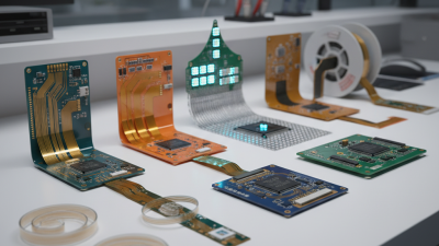
A PCB circuit board is a flat platform that connects electronic components through designed copper paths. Its base usually contains fiberglass, resin, copper layers, solder mask, and printed markings. Components sit on pads, while vias connect different layers. When power enters, traces guide current to resistors, processors, sensors, or connectors. Signals travel along controlled routes, not through loose wires.
This structure makes products smaller, repeatable, and easier to manufacture. It also supports testing because every connection follows a documented layout. A 2024 Fortune Business Insights report estimated the global PCB market at about US$95 billion and projected it to exceed US$145 billion by 2032. The growth reflects demand for compact electronics, vehicles, medical equipment, and communication devices. However, market estimates use different methods. The numbers should not be treated as absolute truth. A PCB can still fail through heat, moisture, vibration, or an overlooked clearance. That weakness deserves attention.
Tips: Define voltage, current, temperature, and board size before layout. Keep high-speed traces short. Separate noisy power paths from sensitive signals. Add test points where repair access matters. Choose the layer count carefully; more layers improve routing, but they raise cost and manufacturing risk. A prototype may work on the bench, yet fail during long operation. Thermal testing and inspection remain necessary.
Why Choose a PCB Circuit Board for Your Project?
A printed circuit board (PCB) provides a compact, repeatable way to mechanically support components and electrically connect them through copper traces, vias, and solder joints. Copper weight is commonly used to specify the approximate thickness of the copper foil on a PCB.
How to read the chart: One ounce of copper is approximately 35 micrometres (µm) thick. Heavier copper layers provide more conductive material and can support higher current capacity, while standard copper weights are suitable for many general electronic circuits.
Which Project Requirements Make a PCB a Suitable Choice?
A PCB becomes suitable when a project needs stable connections, repeatable assembly, and controlled use of space. In bench testing, I have seen loose wires turn a simple sensor prototype into a debugging exercise. A board replaces that uncertainty with defined traces, mounting points, and labeled test pads. It also keeps signal paths shorter. That matters for fast digital signals and low-level analog measurements.
Project volume and physical limits also guide the decision. A compact enclosure may leave no room for hand-wired harnesses. A PCB can place connectors, controllers, sensors, and protection parts on one measured layout. Choose it when the design will be assembled more than once, because consistent routing reduces variation between units. It is less convincing for a single rough prototype. A breadboard may be faster there. This is where judgment matters.
Electrical and environmental requirements deserve careful review. Check current capacity, heat, vibration, moisture, insulation distances, and service access before approving the layout. Add mounting support, strain relief, and test points if technicians must inspect the product. I once underestimated connector access, and a working board became awkward to repair. That mistake was avoidable. Clear schematics, documented tests, and verified measurements make the design more reliable.
How Does PCB Design Improve Circuit Performance and Reliability?
A PCB circuit board improves performance by giving every component a controlled physical relationship. During board reviews, I have seen short signal paths reduce noise and timing errors. Careful routing also limits unwanted capacitance and inductance. This matters in compact controllers, sensor units, and communication equipment. A solid ground plane can provide a quieter return path. It can also reduce electromagnetic interference around sensitive traces.
Reliability depends on more than schematic accuracy. Designers must check trace width, copper thickness, spacing, and operating temperature. Thermal vias can move heat away from power components. Mounting holes and connector positions also need mechanical verification. Testing prototypes under vibration, heat, and repeated power cycles reveals weaknesses early. Still, no layout is perfect. One overlooked clearance can delay production. Design reviews should challenge assumptions, not merely confirm them.
Tips: Keep high-speed traces short and direct. Separate noisy power paths from delicate analog signals. Add test points where measurements are practical. Review the board with manufacturing and assembly limits in mind. A small revision may improve long-term reliability more than an expensive component change. I sometimes prefer a slightly larger board when it provides cleaner routing, easier inspection, and safer thermal margins. That choice is not always elegant, but it is often more dependable.
How Can You Evaluate PCB Cost, Production, and Maintenance Needs?
Choosing a PCB circuit board starts with a realistic cost review, not the lowest quotation.
Ask for a complete cost breakdown. Include laminate, copper weight, layer count, drilling, surface finish, tooling, testing, shipping, and engineering changes.
A four-layer board may cost more than a two-layer board, but it can reduce wiring, noise, and assembly time.
IPC production guidance emphasizes measurable design rules, inspection criteria, and process control.
Request the supplier’s first-pass yield, defect categories, and electrical test coverage.
Low yield can erase an attractive unit price.
Panel utilization also matters. A board that leaves large empty spaces wastes material.
However, I still find early estimates imperfect. Small changes in via size or impedance requirements can shift the quotation sharply.
Maintenance deserves equal attention.
Select accessible test points, clear reference markings, replaceable connectors, and materials rated for the operating temperature.
The Global E-waste Monitor 2024 reported 62 million tonnes of electronic waste in 2022, with only 22.3% formally collected and recycled.
Longer service life reduces replacement pressure. Plan inspection intervals around heat, vibration, moisture, and current load.
A 2024 global smart-manufacturing survey found that 86% of manufacturers viewed smart production as a major competitiveness priority.
Add traceability, revision control, and repair records from the first production batch.
It costs little then. Retrofits are rarely cheap.