Printed circuit boards rarely attract attention, yet they connect the components inside phones, medical devices, vehicles, and data-center servers. Their manufacture demands precise layer alignment, controlled copper thickness, clean drilling, and dependable inspection. Small details matter. A minor defect can disrupt an entire assembly.
Prismark’s 2024 industry review reported a 15% contraction in global PCB production value during 2023 and forecast a 5.8% rebound in 2024. Those shifts underline how closely demand follows electronics markets. Industry analyst Dr. Hayao Nakahara has described the sector as “a barometer of the electronics industry.” That is a useful lens, though market growth alone cannot identify the right supplier.
This guide examines ten printed circuit board manufacturing companies through practical criteria: production capabilities, engineering support, quality processes, regional reach, and the markets they serve. Some excel at rapid prototypes; others handle complex multilayer boards or high-volume orders. Compare the details: stated tolerances, certifications, traceability, and how clearly each company explains its process. Fit matters more. A prominent name may not suit a small, specialized project, and a broad capability list does not prove consistent performance. Use this shortlist as a starting point, then verify claims directly with each manufacturer.
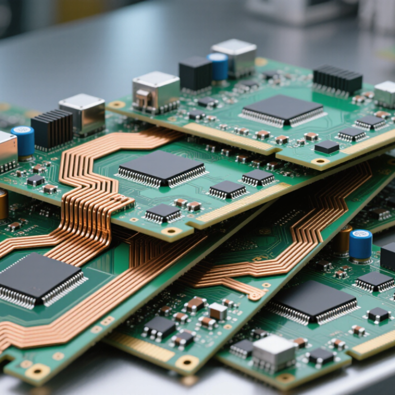
Printed circuit board manufacturing companies turn electrical designs into physical boards that hold and connect electronic components. Their products range from simple, single-layer boards to complex multilayer circuits. A finished bare board may contain a fiberglass or other substrate, thin copper traces, drilled holes, and plated vias that link layers. A solder mask protects exposed copper, while small printed labels help identify component locations. These details matter. A misplaced hole can disrupt assembly.
Some manufacturers also produce assembled circuit boards. They place components onto the board and solder them using processes suited to the design and parts. Others focus on fabrication and ship bare boards for a separate assembly step. Capabilities vary, so buyers should check whether a supplier handles prototypes, repeat production, testing, or assembly. Ask about layer count, board thickness, copper weight, and surface finish. Specifics help. A board for a compact sensor may need narrow traces and tiny vias, while a power-control board may need thicker copper to carry more current. Specifications do not tell the whole story, though; real-world performance can depend on layout, materials, and assembly quality. Even a clear drawing may leave room for interpretation.
This chart shows approximate nominal copper thicknesses commonly used in PCB fabrication. It describes material specifications, not manufacturer rankings or company-specific capabilities.
Approximate values use the common convention of about 35 μm of copper per oz/ft². Finished copper thickness can vary with the foil and plating process.
Printed circuit boards begin as digital layouts that define copper paths, component positions, and connection points. Engineers review these files for spacing, current needs, and manufacturing limits before production starts. A thin copper layer is bonded to a rigid or flexible insulating material. Photoresist and controlled light transfer the circuit pattern onto the surface. Unwanted copper is then etched away, leaving conductive traces behind. Small details matter.
For multilayer boards, manufacturers stack patterned sheets with insulating material between them. Heat and pressure bond the layers into one panel. Drilling creates holes for component leads and connections between copper layers. Plating coats these holes with copper, forming electrical pathways through the board. Even slight misalignment can affect a finished board, so layer registration needs careful checks.
A solder mask covers most exposed copper and helps prevent accidental solder bridges during assembly. Screened markings identify component locations, while a chosen surface finish protects exposed pads. The panels are cut to shape, then inspected for defects. Electrical testing checks whether connections match the design. Visual inspection can catch scratches or uneven coating, though it cannot reveal every hidden flaw. Manufacturing choices vary with board thickness, layer count, and intended use; a process suited to a simple control board may not fit a dense, heat-sensitive design. Teams sometimes discover that a file needs revision only after a test panel exposes a practical issue.
Choosing a PCB manufacturer starts with matching its capabilities to your board, not comparing prices alone. Ask whether it routinely handles your layer count, copper weight, board thickness, and minimum trace spacing. Request a capability sheet, then compare its figures with your design files. Check how it controls drilling, plating, lamination, and solder-mask registration. Small differences can affect fit inside a tight enclosure. Ask how defects are recorded and whether test results can be linked to a production lot. Details matter.
A useful reality check is a sample run or first-article inspection before ordering larger quantities. Review the finished boards for clean edges, consistent plating, readable markings, and accurate dimensions. Ask about electrical testing, inspection steps, and how engineering questions are handled when files conflict. Quick replies help, but precise answers matter more. Not every supplier will suit every project. That can be frustrating. Confirm that any quality certifications apply to the facility and processes you will actually use. Compare lead times, shipping assumptions, tooling charges, and remake policies in writing. The lowest quote may exclude useful checks, while the most polished sales response proves little about shop-floor control. I would also leave room for a second review; even experienced teams miss things.
Ten notable PCB manufacturing companies are best compared by capability, not by a universal ranking. A 2024 global market forecast from Prismark estimated PCB production value at about US$73.9 billion, while noting uneven growth across product categories. That scale matters. A supplier making millions of multilayer boards may not suit a team needing a small prototype run. A useful shortlist covers ten specialties: high-volume multilayer, HDI, flexible, rigid-flex, quick-turn prototypes, automotive, medical, RF, heavy-copper, and regional low-volume production.
Ask each manufacturer for evidence tied to your actual design. Check layer count, minimum trace width, microvia structure, copper weight, and achievable tolerances. Request sample inspection data, electrical-test coverage, and a clear explanation of how defects are handled. For a six-layer board, a cross-section image can reveal whether the finished stack-up matches the drawing. Ask about lead times for both standard and complex builds. Trade-offs matter. No shortlist is perfect. A low quoted price can conceal tooling charges or limited process controls, while a strong certification list does not guarantee a suitable production line. Compare like-for-like quotes and review recent, relevant quality records before choosing.
A brand-neutral overview of ten established PCB manufacturing categories and their typical capabilities. This is not a company ranking; specifications vary by fabricator and design.
| No. | Manufacturing Category | Typical Construction | Common Materials | Typical Applications | Key Design Consideration |
|---|---|---|---|---|---|
| 1 | Single-Sided Rigid Boards | One conductive copper layer on a rigid insulating substrate | FR-4, paper-phenolic laminates | Simple controls, basic consumer products, LED products | Suitable for lower-complexity layouts; component routing is limited to one copper side. |
| 2 | Double-Sided Rigid Boards | Two copper layers connected by plated through-holes | FR-4 and other glass-reinforced epoxy laminates | Power supplies, instrumentation, industrial controls | Via placement and copper clearances affect routing and manufacturability. |
| 3 | Standard Multilayer Boards | Three or more copper layers laminated with insulating dielectric layers | FR-4, high-Tg epoxy laminates | Computers, communications equipment, automotive electronics | Layer stack-up, impedance needs, and thermal design should be agreed with the fabricator. |
| 4 | High-Layer-Count Boards | Many copper layers in a laminated rigid-board stack-up | FR-4 and specialized low-loss laminates | Networking equipment, servers, complex industrial systems | Registration, lamination, signal integrity, and board thickness require careful planning. |
| 5 | High-Density Interconnect (HDI) Boards | Fine-line circuitry with microvias; may use sequential lamination | FR-4 and thin dielectric materials suitable for HDI construction | Compact mobile devices, wearables, dense computing modules | Microvia structure, via reliability, and minimum feature limits must match the chosen process. |
| 6 | Flexible Circuit Boards | Patterned copper on a bendable dielectric film | Polyimide films and rolled-annealed copper | Compact electronics, cameras, displays, moving assemblies | Bend radius, copper type, and the location of bends influence service life. |
| 7 | Rigid-Flex Boards | Rigid PCB sections joined by flexible circuit sections | Rigid laminates combined with polyimide flex layers | Aerospace equipment, medical instruments, compact enclosures | Transition zones and bend regions need mechanical and stack-up review. |
| 8 | RF and Microwave Boards | Controlled-impedance construction for high-frequency signals | Low-loss PTFE-based or other RF-grade laminates, sometimes hybrid stack-ups | Antennas, radar systems, wireless and satellite equipment | Material properties, dielectric thickness, copper profile, and impedance tolerances matter. |
| 9 | Metal-Core Boards | Conductive metal base with an electrically insulating dielectric and copper circuitry | Aluminum or copper base with thermally conductive dielectric | LED lighting, power conversion, heat-generating electronics | Thermal performance depends on the dielectric layer, base material, and mounting conditions. |
| 10 | Ceramic Substrate Boards | Conductive patterns formed on ceramic insulating substrates | Alumina, aluminum nitride, and other technical ceramics | Power electronics, high-temperature assemblies, specialized RF modules | Ceramic selection affects thermal conductivity, electrical insulation, and mechanical behavior. |
Choosing a PCB manufacturer starts with the board’s actual requirements, not a polished sales page. Define the layer count, dimensions, copper weight, finish, and expected order volume before requesting quotes. A supplier’s capabilities should match your design tolerances and production needs. Ask whether engineers review files for manufacturing risks before fabrication.
Details matter. Request clear information about inspection, electrical testing, material traceability, and how defects are handled. For example, a prototype with fine-pitch components may need tighter registration and closer inspection than a simple control board. Check lead times against your build schedule, and confirm whether quoted dates include shipping. A low price can lose its appeal if unclear specifications trigger revisions.
For early builds, ask how easily quantities can scale from prototypes to repeat orders. Compare quotes using the same board files and specifications; otherwise, the numbers may not be comparable. Not always. A manufacturer with the shortest lead time may not offer the support your design needs. One overlooked detail is communication: unclear answers about tolerances or test coverage deserve follow-up. Even careful teams sometimes submit files before the design is stable. Review the final stack-up and fabrication notes before approving production.