
How to Choose Printed Circuits for Your Project?
Choosing printed circuits is not simply a matter of counting layers or comparing prices. The right board must match electrical performance, mechanical space, heat, production volume, and compliance requirements. A prototype that works on a laboratory bench may fail inside a sealed industrial enclosure. Small details matter, including trace width, copper thickness, connector placement, and surface finish.
Industry data shows why this decision deserves careful planning. Grand View Research estimated the global printed circuit board market at approximately USD 89.7 billion in 2023, with continued growth expected through 2030. IPC’s PCB Industry Results reports also track bookings, sales, and book-to-bill trends across the sector. These indicators suggest stronger demand, but they do not remove engineering risks. Supply availability, material substitutions, and fabrication capacity can still change project costs quickly. Market reports provide direction, not a complete design answer.
A practical selection process should begin with the project’s real operating conditions. Will the circuit face vibration, moisture, rapid temperature changes, or high current? A four-layer FR-4 board may suit a control unit, while a metal-core board may better support high-power LEDs. Flexible circuits can fit a moving hinge, but repeated bending requires tested bend radii. Cost alone is a weak guide. I have seen inexpensive boards create expensive rework through poor thermal paths and difficult assembly. That lesson is easy to overlook. Designers should compare supplier capabilities, testing records, material certifications, and lifecycle support before approval. The best choice is rarely the cheapest board; it is the board that remains reliable when the project leaves the drawing table.
Understanding Printed Circuit Types and Their Applications
How to Choose Printed Circuits for Your Project?
Understanding Printed Circuit Types and Their Applications
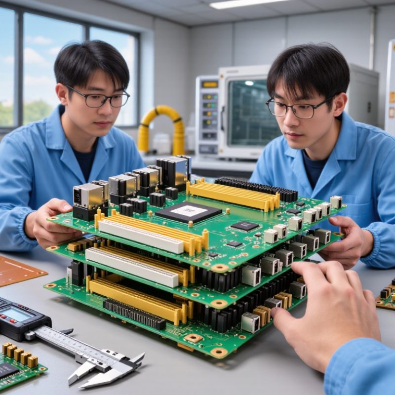
Printed circuit boards differ in structure, cost, flexibility, and heat performance. Single-sided boards suit simple controls, indicator panels, and low-density devices. Double-sided boards support more connections without a major size increase. Multilayer boards manage dense routing in computers, instruments, and industrial controllers.
Choose based on the working environment.
High-density interconnect boards use finer traces and microvias. They fit compact products, but manufacturing tolerances become less forgiving. Flexible circuits bend around hinges and narrow spaces. Rigid-flex designs combine stable mounting areas with movable sections. A small wearable device may need this combination, while a factory controller usually benefits from a rigid multilayer board.
Market data shows why these options matter. The 2024 Global Printed Circuit Board Market report from Mordor Intelligence estimated the market at about USD 76 billion in 2024. It also identified multilayer boards as a major product segment. Grand View Research reported strong growth in flexible printed circuits, driven by mobile, medical, and automotive applications.
Thermal demands deserve equal attention. Copper weight, board thickness, and via design affect heat movement. A board that works on a test bench may fail inside a sealed metal enclosure. I once underestimated connector stress on a compact layout. The circuit passed electrical testing, yet repeated bending damaged the solder joints. Reviewing IPC-2221 guidance, airflow, assembly limits, and service access can prevent that mistake. Sometimes, the smallest board is not the best board.
How to Choose Printed Circuits for Your Project? - Understanding Printed Circuit Types and Their Applications
| Printed Circuit Type | Typical Construction | Main Advantages | Limitations | Suitable Applications | Design and Selection Considerations | Relative Cost |
|---|---|---|---|---|---|---|
| Single-Sided PCB | One conductive copper layer bonded to an insulating substrate, usually with components mounted on one side. | Simple layout Easy manufacturing Short lead time Low cost | Limited routing space and lower circuit density; crossing traces generally require jumpers or additional wiring. | Basic power supplies LED lighting Simple control panels Consumer appliances | Choose this type when the circuit is electrically simple and board area is available for wider routing paths. | Very low |
| Double-Sided PCB | Two copper layers separated by an insulating dielectric, with plated through-holes connecting selected traces between layers. | Higher routing density Compact layout Better design flexibility | More complex than a single-sided board and usually requires plated through-hole processing. | Industrial controls Instrumentation Motor controllers Embedded systems | Use when the design needs additional routing capacity but does not require the density or signal isolation of multiple internal layers. | Low |
| Multilayer PCB | Three or more copper layers laminated with insulating dielectric layers; internal planes may be used for power, ground, and signal routing. | High circuit density Improved signal integrity Better power distribution Compact size | Higher fabrication cost, longer production time, and more demanding stack-up and impedance-control requirements. | Computing equipment Networking hardware Medical electronics Advanced control systems | Select the layer count based on routing requirements, controlled impedance, power integrity, thermal needs, and component density. | Moderate to high |
| Rigid PCB | Built on a solid, non-flexible substrate that maintains a fixed shape during installation and operation. | Mechanical stability Consistent dimensions Wide material availability Good component support | Cannot be bent during normal use; unsuitable for assemblies requiring repeated flexing or tight three-dimensional routing. | Control boards Computers Test equipment Household electronics | Choose a rigid board when the enclosure provides a fixed mounting surface and the assembly does not need dynamic movement. | Low to moderate |
| Flexible PCB | Conductive layers formed on a flexible polymer substrate, allowing the circuit to bend or fold within specified limits. | Lightweight Space saving Reduced wiring Dynamic routing | Requires careful bend-radius control and strain relief; assembly and material costs may be higher than for rigid boards. | Wearable devices Compact displays Cameras Moving assemblies | Verify minimum bend radius, bend cycles, stiffener requirements, connector locations, and mechanical stress points. | Moderate to high |
| Rigid-Flex PCB | A combined structure containing rigid board sections connected by flexible circuit sections in one integrated assembly. | High packaging flexibility Fewer connectors Improved reliability Three-dimensional routing | More difficult to design, manufacture, inspect, and repair; material and tooling costs are typically higher. | Aerospace systems Compact instruments Portable electronics High-reliability equipment | Use when space, weight, connector reduction, or repeated assembly movement justifies the additional engineering complexity. | High |
| Metal-Core PCB | A circuit board using a metal base, commonly aluminum or copper, beneath the dielectric to improve heat spreading. | Enhanced thermal management Mechanical strength Reduced hot spots | Limited suitability for certain multilayer structures and electrically conductive mounting surfaces require proper isolation. | High-power LED lighting Power converters Automotive electronics Motor drives | Evaluate heat generation, thermal resistance, mounting method, dielectric isolation, and the need for a heatsink or chassis interface. | Moderate to high |
| High-Frequency PCB | Uses low-loss dielectric materials and controlled geometry to support high-frequency or high-speed signal transmission. | Lower signal loss Controlled impedance Stable high-speed performance | Material selection, fabrication tolerances, surface finish, and stack-up control are more demanding. | Wireless communication Radar systems RF test equipment High-speed data links | Consider operating frequency, dielectric constant, dissipation factor, trace geometry, loss budget, and impedance requirements. | High |
| HDI PCB | High-density interconnect construction using fine traces, microvias, and compact component spacing to increase routing density. | Very high density Smaller form factor Shorter interconnects Advanced packaging | Requires advanced fabrication and inspection capabilities; design rules and manufacturing tolerances are more restrictive. | Mobile electronics Miniature medical devices Compact computing systems Fine-pitch packages | Confirm microvia structure, sequential lamination needs, minimum feature sizes, component pitch, and assembly yield targets. | Very high |
Related Posts
-

Why Choose a PCB Circuit Board for Your Project?
-
What Are the Best Printed Circuit Boards in China?
-
What Is Production PCB and How Can Buyers Source It?
-

Why Is PCB Production Important for Global Buyers?
-
How to Find a Fast PCB Manufacturer?
-

2025 Strategies for PCB Prototyping to Improve Product Development Efficiency