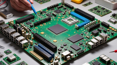
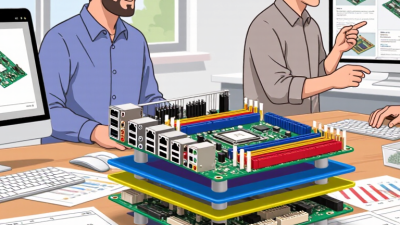
What Are the Top Circuit Board Design Types in 2026? The answer depends on the product, not a passing trend. A compact wearable may need a flexible circuit, while an industrial controller often benefits from a rigid board. High-speed links, heat, vibration, and enclosure space all change the choice. Small details matter. A connector that shifts by a few millimeters can reshape the layout.
Signal-integrity educator Dr. Eric Bogatin has said, “The only way to learn about signal integrity is to do it.” That practical mindset suits circuit board design in 2026. Rigid, flexible, and rigid-flex boards remain important. High-density interconnect designs support tighter component spacing, while metal-core boards help move heat away from power components. High-frequency and advanced package-substrate designs serve more specialized needs. Each type solves a different problem. None is automatically best.
This guide compares the leading options by structure, applications, strengths, and trade-offs. It also considers manufacturability, material choice, and testing—not just routing density or board size. Imagine a small board beneath a warm processor, with a narrow connector and little airflow. The right design must work there, not only in a CAD view. Forecasts for 2026 can miss real production constraints. That deserves a second look. Designers should confirm supplier capabilities and validate assumptions with prototypes before committing to a final layout.
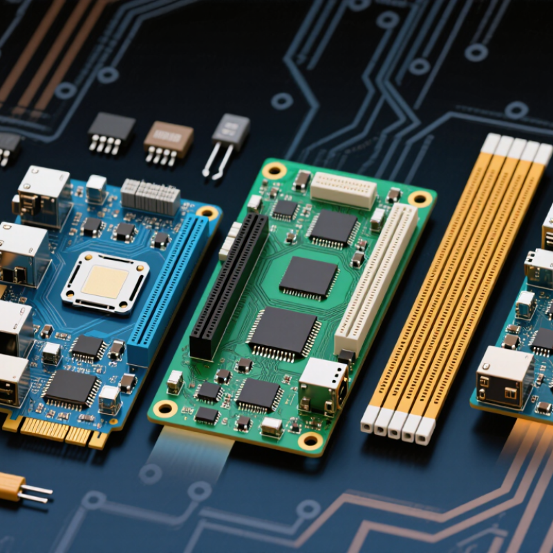
Rigid PCBs remain a practical choice for electronics that need predictable support and repeatable assembly. Their solid substrate helps components stay aligned when a device is handled or mounted inside an enclosure. In a typical design review, engineers check board thickness, copper weight, component spacing, and mounting-hole positions together. These details affect fit and production yield. A well-planned rigid board can also simplify assembly by keeping connectors and test points accessible. Small details count.
Cost control starts with sensible choices, not simply the cheapest material. A common layer stack, adequate trace widths, and fewer unusual drill sizes can make fabrication more straightforward. Thermal paths deserve attention too: a power component placed far from a copper area may run hotter than expected. Rigid boards are not ideal for every moving or tightly curved product. That trade-off is easy to overlook. A stable design still needs testing under its actual load and operating temperature.
Multilayer PCB design gives engineers more room to separate signals, power, and ground. A six- or eight-layer stack can place reference planes close to high-speed traces, helping control impedance and provide shorter return paths. That matters. Grand View Research estimated the global PCB market at USD 76.12 billion in 2023 and projected 5.7% annual growth from 2024 to 2030. The estimate reflects broad demand, not multilayer boards alone, but it underscores the need for reliable design choices.
In a dense control board, for example, a continuous ground plane beneath a differential pair can reduce interference. Power planes can also distribute current across the board, though narrow necks and poorly placed vias may create local voltage drops. Designers should review stack-up, trace geometry, via transitions, and decoupling together—not as isolated tasks. A plane split under a signal path can interrupt its return current and increase noise. Small details matter.
More layers are not automatically better. Extra layers add fabrication cost and can complicate drilling, registration, and thermal management. A four-layer prototype may outperform a poorly planned eight-layer board. That is easy to overlook. Before layout, define target impedance, current demand, connector locations, and manufacturing limits with the fabricator. Then verify critical nets with field-solver tools and physical testing. Simulation helps, but it does not erase uncertainty; real materials and assembly tolerances still vary.
HDI PCB design is becoming essential as processors, memory, and radio components crowd smaller devices. Prismark’s 2024 global PCB industry forecast valued worldwide production at roughly US$73 billion, reflecting the scale of demand for increasingly compact boards. HDI uses fine traces, microvias, and sequential lamination to connect dense component packages without expanding the board. Shorter interconnects can also reduce parasitic effects, helping preserve signal quality at high data rates. Every millimeter matters.
For a dense, high-speed design, start with the component escape routing and layer stackup together. A laser-drilled microvia can connect a fine-pitch pad to an inner layer, while controlled impedance and a continuous reference plane support predictable signal behavior. IEEE 802.3ck specifies Ethernet signaling at 100 gigabits per second per lane, illustrating why routing geometry and return paths deserve early attention. But HDI is not a free upgrade. Extra lamination cycles raise fabrication complexity, and poorly placed vias can still create discontinuities. I have seen teams focus on shrinking traces before checking whether their chosen fabricator can reliably build the stackup. That is a costly assumption. Check via aspect ratios, material properties, and test access with the fabricator before layout is frozen.
In 2026, flexible PCB design is a practical choice for products that bend, fold, or move during use. Think of a fitness band wrapping around a wrist, or a compact camera hinge opening hundreds of times. A flexible circuit can follow that motion while reducing bulky wire bundles. Space matters.
Reliable designs start with the bend, not the outline. Engineers estimate the bend radius, identify whether movement is occasional or continuous, and keep sensitive traces away from sharp folds. Copper thickness, coverlay, and layer count affect durability and cost. A connector can also become the weak point. Small details matter.
Prototypes should be flexed inside the real product, at its actual temperature and speed. Check for cracked traces, lifted pads, and intermittent signals after repeated cycles.
A design that passes a bench test may still fail inside a tight enclosure. That gap is easy to underestimate.
Flexible boards are not automatically better: they need careful support, strain relief, and assembly controls. Sometimes a short rigid-flex section is more sensible than making the whole board flexible. The right trade-off depends on movement, service life, and available space.
Rigid-flex PCB design connects rigid component areas with flexible circuits, creating one assembly that can fold through three dimensions. It can reduce connector count and free space inside compact products. The benefit is tangible: a camera module may wrap around a frame instead of relying on several small boards and cable links. Fewer parts, but tighter design constraints.
The transition between rigid and flexible regions needs careful attention. Copper layers, adhesive thickness, and bend radius affect reliability. Place components and plated vias away from repeated bend zones whenever possible. A sharp fold near a solder joint can concentrate strain, even when the board looks fine after assembly. Looks can mislead.
Three-dimensional layout should be checked against the finished enclosure, not only a flat CAD view. Account for bend direction, clearance, assembly access, and heat from nearby components. Signal paths also need review; a folded route can change spacing and impedance. Simulation helps, but a physical prototype often reveals awkward folds that software misses. That part is easy to underestimate. Test the intended bend cycle and inspect the copper near transitions before committing to production. An early prototype may expose a routing choice that seemed elegant on screen but proves difficult to assemble.
A structural comparison of common PCB types by the rigid and flexible regions used in a single board design.
Rigid-flex designs combine rigid and flexible board regions in one interconnected structure, making them suitable for compact assemblies that fold or fit across multiple planes. The bars show region types, not layer counts or performance ratings.